VP536E View Datasheet(PDF) - Zarlink Semiconductor Inc
Part Name
Description
View to exact match
VP536E Datasheet PDF : 14 Pages
| |||
VP536E
Master Reset
The VP536E can be initialized with the RESET pin. This
is an active low signal and must be active for a minimum of 2
CLK12I clock periods in order for the VP536E to be reset.
Video Timing Reset
The VP536E also features the ability to independently
reset the video timing generator without affecting the data
path. The TSURST pin controls this function. Taking this pin
high resets the video timing generator. If this pin is left open,
it is internally pulled low.
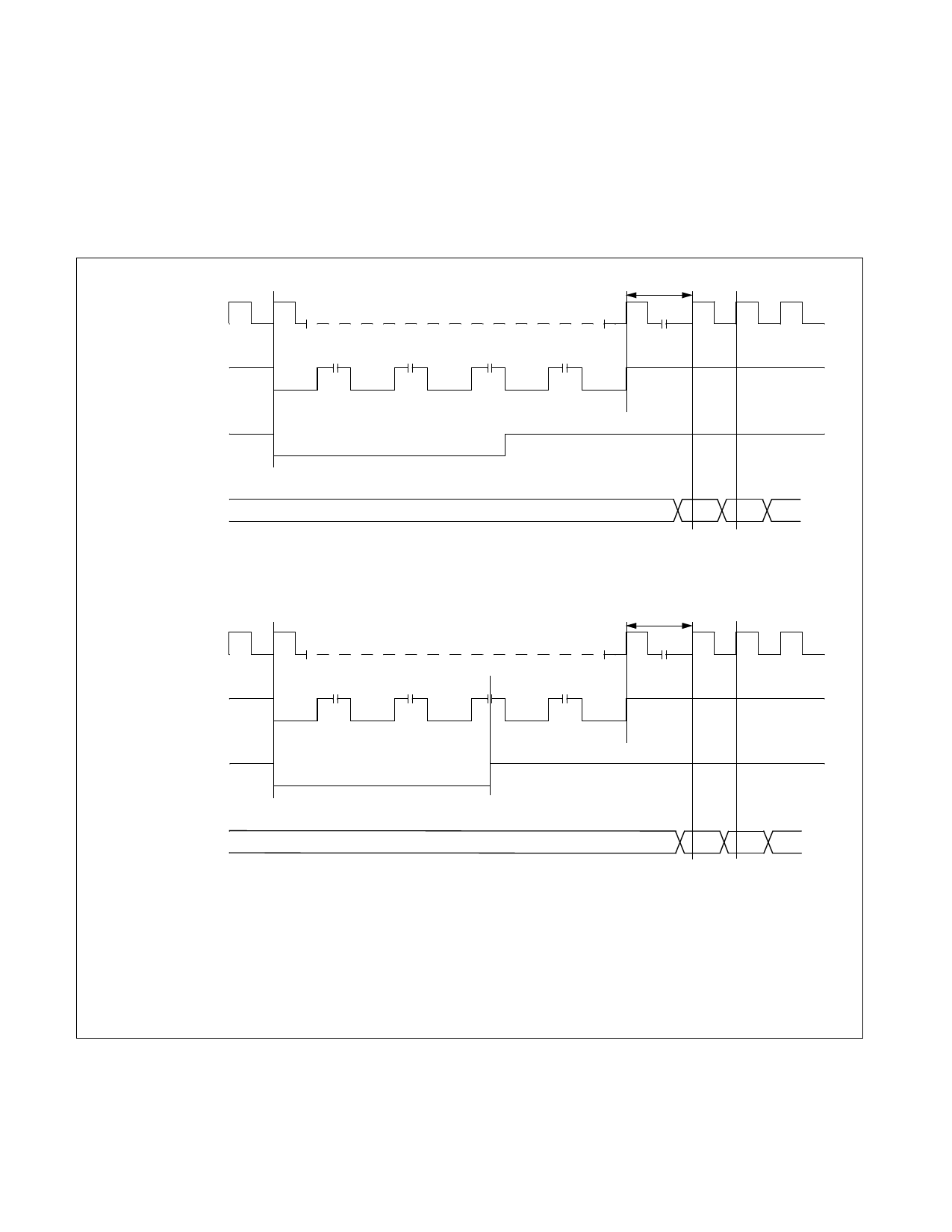
CLK12I
HS
VS
RGB/YUV
INPUT DATA
48 Periods
Line 1
Line 2
Line 3
Line 4
Line 17
Fig. 2a. NTSC Input Timing Diagram
Field 1
Line 17
1st
pixel
2nd
pixel
CLK12I
58Periods
HS
VS
RGB/YUV
INPUT DATA
Line 1
Line 2
Line 3
Line 4
Line 23
Fig. 2b. PAL Input Timing Diagram
Field 1
Line 23
1st
pixel
2nd
pixel
NOTE:
1. Coincident falling edges of HS and VS denote the start of an odd field.
2. VS is low during the first 3 lines in each NTSC field and during the first 21/2 lines in each PAL field.
3. Input pixel data is ignored during composite blanking periods.
4
Share Link: 