VP536E View Datasheet(PDF) - Zarlink Semiconductor Inc
Part Name
Description
View to exact match
VP536E Datasheet PDF : 14 Pages
| |||
VP536E
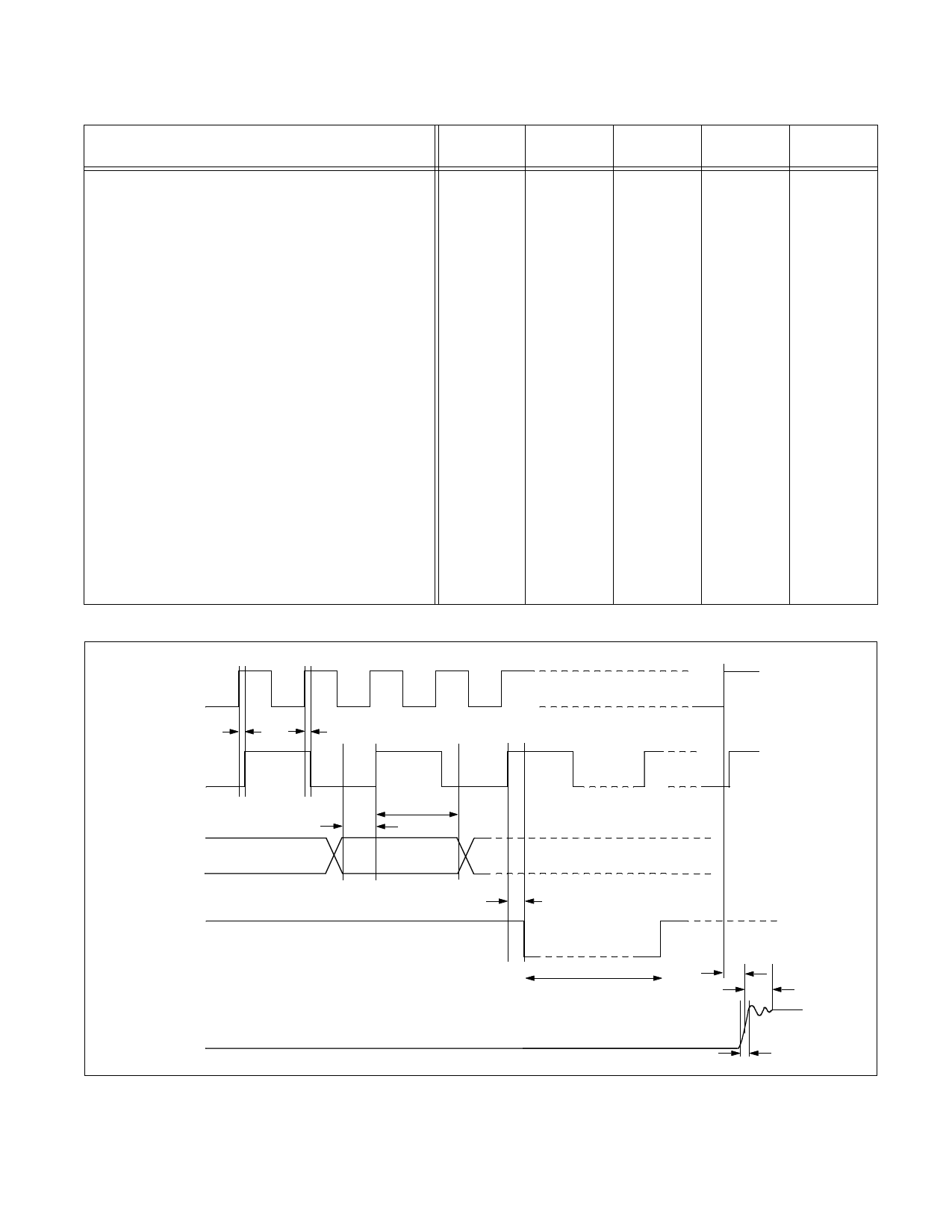
AC Characteristics (see note on Page 11)
Parameter
CLK12I clock delay with respect to CLK25I clock
(tested with 50% duty cycle CLK12I and CLK25I clocks)
Data set-up time (wrt CLK12I clock)
Data hold time (wrt CLK12I clock)
HS/VS output delay wrt CLK12I clock
HS low pulse width (NTSC)
HS low pulse width (PAL)
VS low pulse width(NTSC)
VS low pulse width (PAL)
Input clock pulse width high time
Input clock pulse width low time
Analog video output delay (wrt CLK25I clock)
Analog video output rise/fall time
Analog video output settling time (50% to +/- 1 LSB)
Signal related harmonics of DAC outputs for 1MHz.
direct digitally synthesized sine wave
Pipeline delay (data in to analog video out)
VAA supply current
Power supply rejection
(chromacomp, lumacomp = 0.1uF, f = 1 KHz.)
Timing Waveforms
Symbol
tdCLK
tsuDATA
thDATA
tdSYNC
twHS-NTSC
twHS-PAL
twVS-NTSC
twVS-PAL
tdAVO
trfAVO
tsAVO
IAA
Min.
0
8
5
0
16
16
Typ.
59
69
2388
2360
10
8
12
tbd
20.5
200
40
Max.
18
20
Units
ns
ns
ns
ns
CLK12I cycles
CLK12I cycles
CLK12I cycles
CLK12I cycles
ns
ns
ns
ns
ns
dB
CLK12I cycles
mA
dB
CLK25I
CLK12I
RGB
HS/VS
LUMAOUT,
CHROMAOUT,
COMPOUTB
tdCLK
tsuDATA
thDATA
DATA
tdSYNC
ttwwVHSS
Fig. 9. Input/Output Timing Diagram
tdAVO
tsAVO
trfAVO
10
Share Link: 