VP536E View Datasheet(PDF) - Zarlink Semiconductor Inc
Part Name
Description
View to exact match
VP536E Datasheet PDF : 14 Pages
| |||
VP536E
NTSC/PAL Digital Video Encoder
DS4322 - 3.2 August 1997
FEATURES
s Converts RGB data (3x8bits) to analog composite
video and S-video
s Internal video timing generation
s RGB or YUV input modes
s Progressive scanning (non-interlaced fields)
display mode optional
s Separate horizontal and vertical sync outputs
s 68 pin PLCC package
APPLICATIONS
s Multi-media
s Video Games
s PC’s
s Graphics
s Display Adaptors
s Video Effects Processors
DESCRIPTION
The VP536E converts digital RGB data (3x8bits) into
analog NTSC/PAL composite video and S-video signals. The
outputs are capable of driving doubly terminated 75 ohm
loads with standard video levels.
The device will also accept YUV data. Progressive scan
(non-interlaced fields) video display is available in both
NTSC and PAL modes.
The output pixel rate is approximately 7 times Fsc (color
subcarrier frequency) for NTSC (6.6 times Fsc for PAL)
which is approximately 25MHz. Input pixel rate is half this
frequency; approximately 12.5MHz.
All the necessary synchronization signals are generated
internally. Digital horizontal and vertical sync outputs are
available for use by the host system.
The rise and fall times of sync, burst envelope and video
blanking are internally controlled to be within composite
video specifications.
Two 8-bit digital to analog converters (DACs) are used
to convert the digital luminance and chrominance data into
analog signals. An inverted composite video signal is
generated by summing the complimentary current outputs of
each DAC. An internally generated reference voltage
provides the biasing for the DACs.
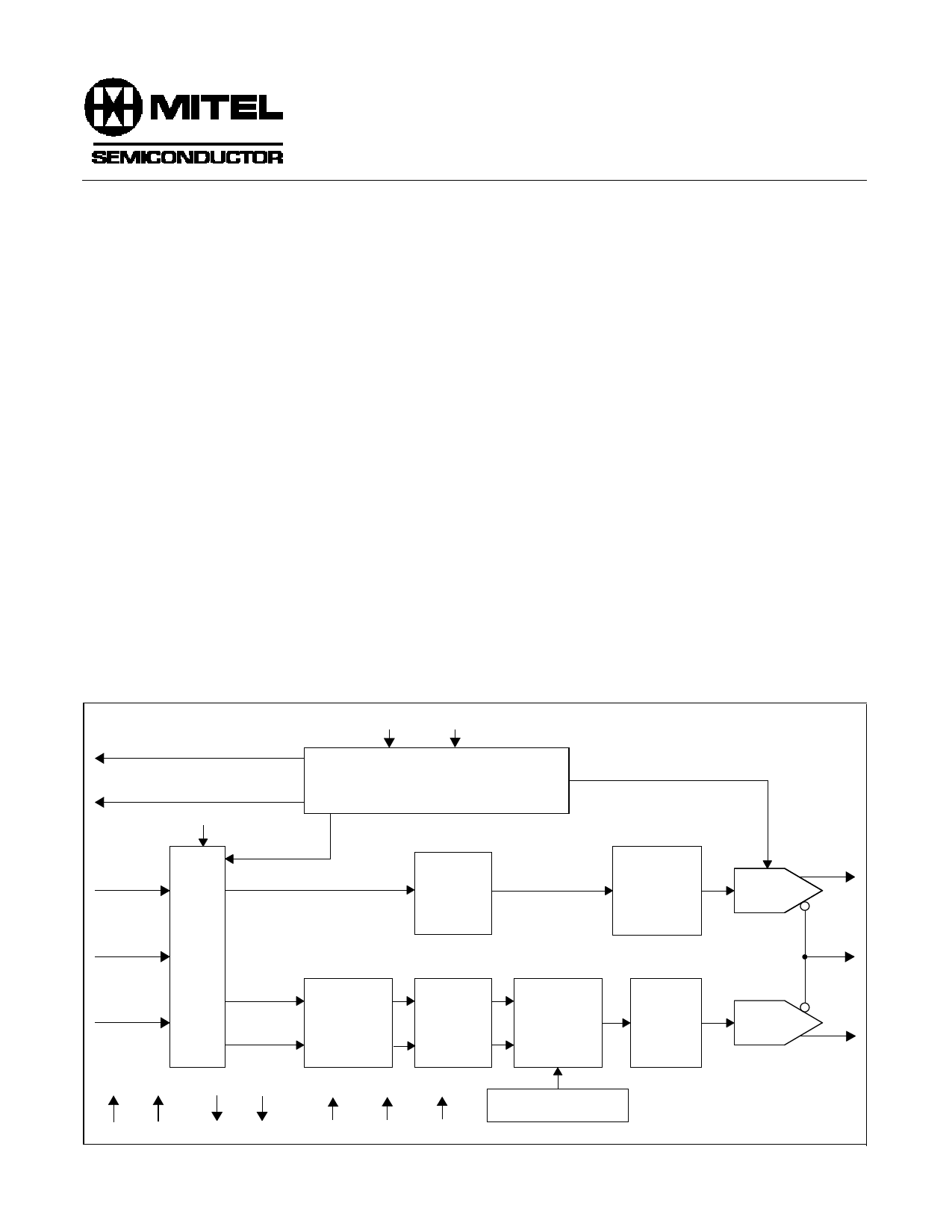
VS
HS
R0:7
G0:7
B0:7
MATRIX
BYPASS
Y
RGB
TO
YUV
MATRIX
U
V
CTRLB1 CTRLB2
VIDEO TIMING GENERATOR
BURST
GATE
INTER-
POLATOR
COMPOSITE SYNC
(SIN X/X)-1
PRECOMPEN-
SATION
LUMA
DAC
LUMAOUT
COMP-
OUTB
CHROMA
LOW-PASS
FILTER
INTER-
POLATOR
MODULATOR
BANDPASS
FILTER
CHROMA
DAC
CHROMAOUT
CLK25I CLK12I CLK25O CLK12O
CTRLA1 CTRLA2 CTRLA3
COLOR SUBCARRIER
GENERATOR
Fig. 1. Functional Block Diagram
Share Link: 