VV5409C001 View Datasheet(PDF) - Vision
Part Name
Description
View to exact match
VV5409C001 Datasheet PDF : 39 Pages
| |||
VV5409 CMOS Monochrome Sensor Datasheet (Restricted) Rev 1.0
3. Automatic Black Level Calibration
Black calibration is used to remove voltage offsets that cause shifts in the black level of the video signal.
VV5409 is equipped with an automatic function that continually monitors the output black level and calibrates
if it has moved out of range. The signal is corrected using two “Black-Calibration” DACs:
1. ADC stage DAC, B0[7:0].
2. OSA Input Offset Compensation DAC, B1 [7:0]
Black calibration can be split into two stages, monitor and update. During the monitor phase the current
black level of 4 black reference lines at the top of the pixel array is compared against two threshold values.
If the current value falls outside the threshold window then an update cycle is triggered. The update cycle can
also be triggered by a change in the gain applied to sensor core or via the serial interface (see also Section
6.6.5).
VV5409 CMOS Monochrome Sensor Datasheet (Restricted) Rev 1.0
4. Exposure Control
The exposure time for a pixel and the gain of the input amplifier to the 8-bit ADC are programmable via the
serial interface. The explanation below assumes that the gain and exposure values are updated together as
part of a 5 byte serial interface auto-increment sequence.
The exposure is divided into 2 components - coarse and fine. The coarse exposure value sets the number of
lines a pixel exposes for, while the fine exposure sets the number of additional pixel clock cycles a pixel
integrates for. The sum of the two gives the overall exposure time for the pixel array.
Exposure Time = Clock Divider Ratio x (Coarse x Line Length + Fine) x (CLKI clock period)
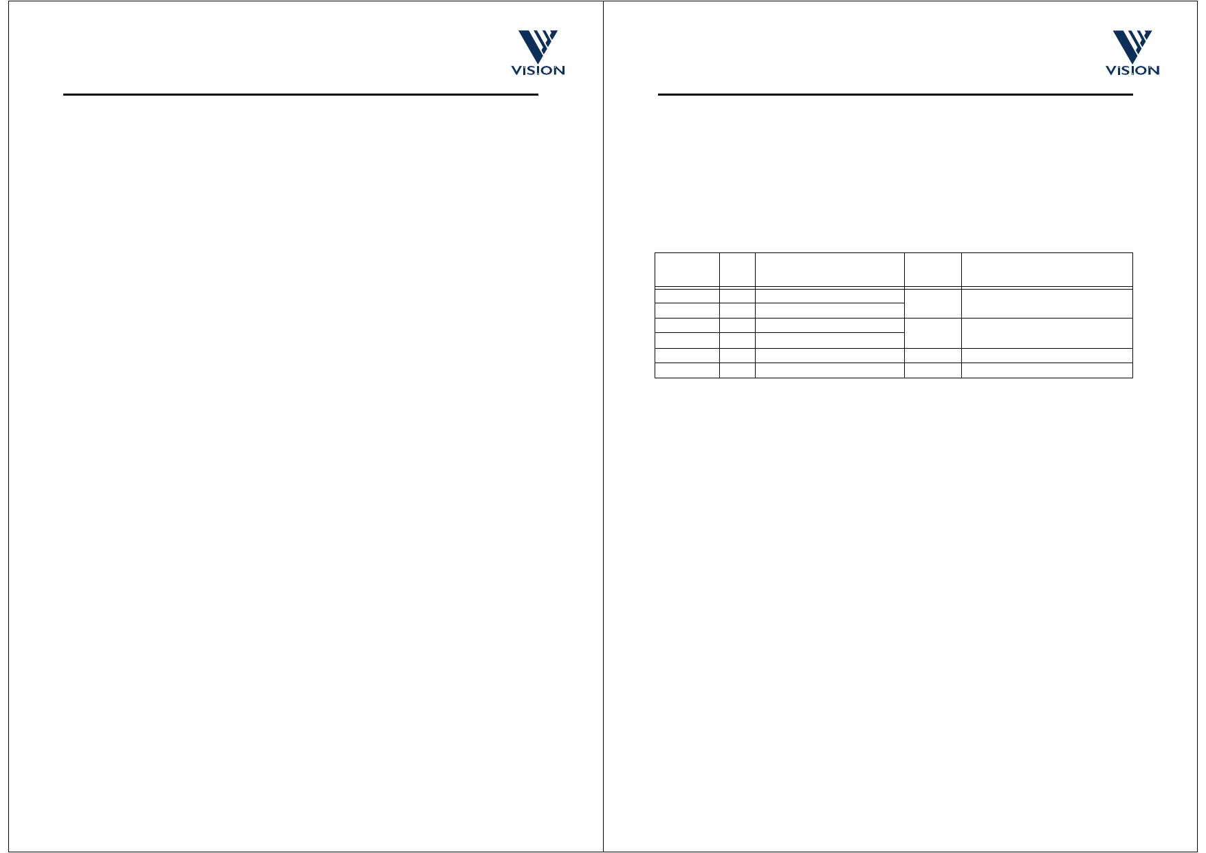
Register
Index
32
33
34
35
36
37
Bits
Function
Default
Comment
0:0 Fine MSB exposure value
7:0 Fine LSB exposure value
0:0 Coarse MSB exposure value
7:0 Coarse LSB exposure value
3:0 Gain value
1:0 Clock divisor value
0
Maximum Line Length Mode
Dependant
302
Maximum equals Field Length-1.
0
0
Table 4.1 : Exposure, Clock Rate and Gain Registers
If an exposure value is loaded outwith the valid ranges listed in the above table the value is clipped to lie
within the above ranges.
Exposure and gain values are re-timed within the sensor to ensure that a new set of values is only applied to
the sensor array at the start of each frame. Bit 0 of the Status Register is set high when a new exposure value
is written via the serial interface but has not yet been applied to the sensor array.
There is a 1 frame latency between a new exposure value being applied to the sensor array and the results
of the new exposure value being read-out. The same latency does not exist for the gain value. To ensure that
the new exposure and gain values are aligned up correctly the sensor delays the application of the new gain
value by one frame relative to the application of the new exposure value.
To eliminate the possibility of the sensor array seeing only part of the new exposure and gain setting, if the
serial interface communications extends over a frame boundary, the internal re-timing of exposure and gain
data is disabled while writing data to any location in the Exposure page of the serial interface register map.
Thus if the 5 bytes of exposure and gain data is sent as an auto-increment sequence, it is not possible for
the sensor to consume only part of the new exposure and gain data.
See also Section 6.6.3.
Commercial In Confidence
Commercial In Confidence
cd38041a.fm
08/10/98
11
cd38041a.fm
08/10/98
12
Share Link: 