VV5409C001 View Datasheet(PDF) - Vision
Part Name
Description
View to exact match
VV5409C001 Datasheet PDF : 39 Pages
| |||
VV5409 CMOS Monochrome Sensor Datasheet (Restricted) Rev 1.0
digitised pixel-data. This value is output, once per line, as part of the embedded “end-of-line” sequence.
While this amplifier is primarily intended as a Microphone amplifier, it can be used as way to digitise any
“slow-moving” analogue input. The maximum sample rate is approximately 15k samples/second as there is
only one sample per line of video. See also Section 9.1.
1.8.2 Debounced Switch Input
This de-bounced input (the FST/DIN pin re-configured as a debounced switch input pin) is designed for use
with a switch, for still-image capture. If the switch is pressed, it sets a flag in the status line for the next field,
marking it as the one the user has selected. See also Section 9.2.
Commercial In Confidence
cd38041a.fm
08/10/98
7
VV5409 CMOS Monochrome Sensor Datasheet (Restricted) Rev 1.0
2. Operating Modes
2.1 Video Timing
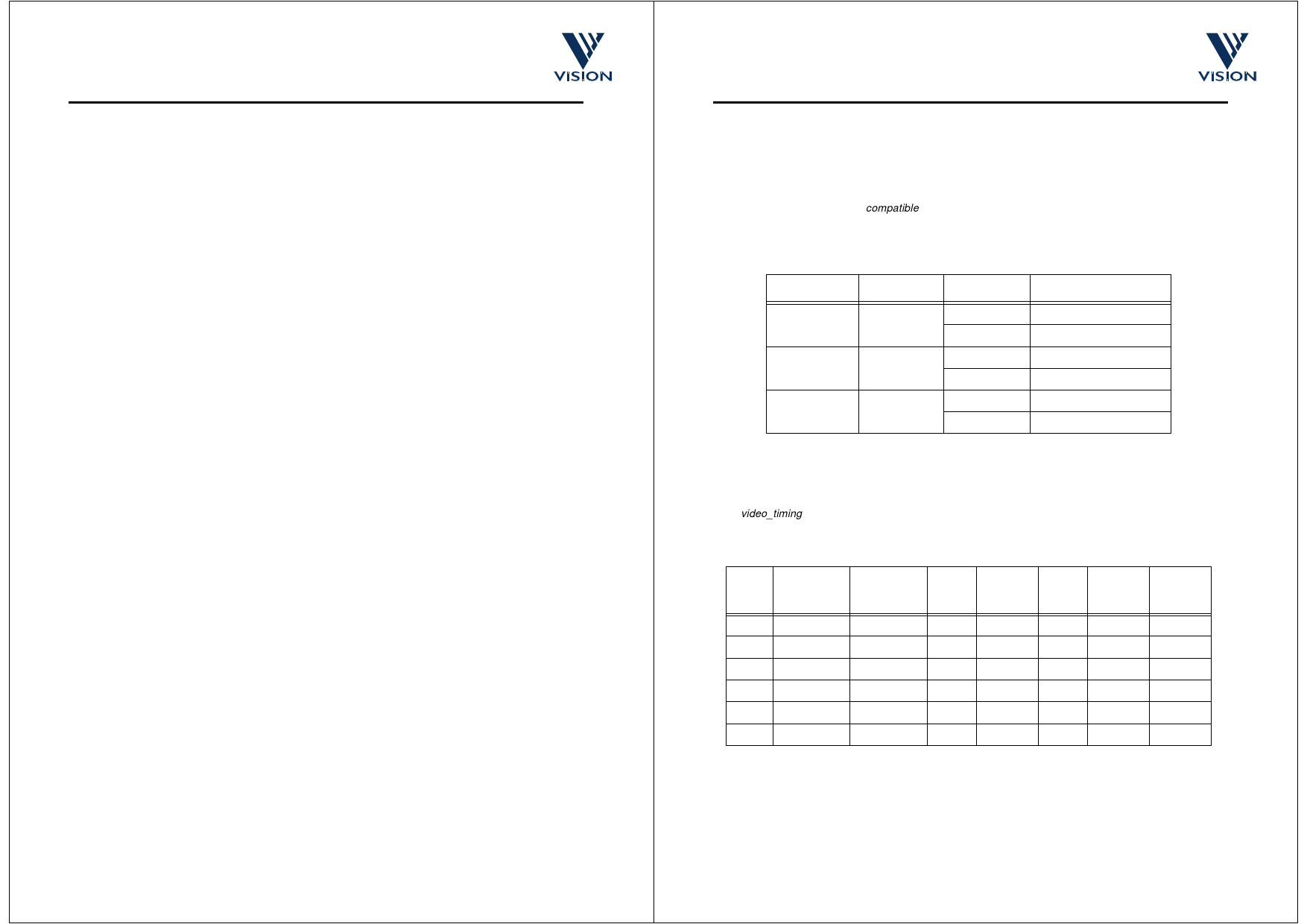
The video format mode on power-up is determined by the value of bits 6-7 of the setup0 register. It may be
desirable to access a larger image array size by enabling PAL or NTSC video output modes. While the video
outout timing from the sensor is compatible with PAL.NTSC/CCIR656 formats, video sync timing and
encoding must be performed by an external host controller.
The frame/field rate is programmable only through the serial-interface. Setup0 bit 3 selects between 30 and
25 frames per second for the CIF modes, and 60/50 fields per second for the Digital, and Analog Timing
modes.
Video Mode setup0[6-7] setup0 Bit3
Video Mode
CIF (VV6404)
002
0
1
CIF - 25 fps
CIF - 30 fps
DIGITAL (CCIR)
012
0
1
PAL (656)
NTSC (656)
ANALOG (TV)
102
0
1
PAL (8 fsc)
NTSC (8 fsc)
Table 2.1 : Video Timing Mode Select Pins
The number of video lines-in for each frame-rate, is the same (304) for each of the CIF modes. The slower
frame rate is implemented, by simply extending the line period from 393 pixel periods, to 471 pixel periods.
Table 2.2 details the setup for each of the video timing modes. Changing either the mode pin, or a serial write
to the video_timing register will force the contents of other registers in the serial-interface to change to the
appropriate values. If, for example, a different data output-mode is required from the default, for a particular
video mode, a write to the appropriate register after the mode has changed will setup the desired value.
Mode Video Mode
0 CIF - 25 fps
1 CIF - 30 fps
2 PAL(656)
3 NTSC (656)
4 PAL (8 fsc)
5 NTSC (8 fsc)
Clock
(MHz)
Pixel
Clock
Divisor
Video
Data
Line
Length
7.15909
2
356 x 292 471
7.15909
2
356 x 292 393
13.500000
2
356 x 292 432
13.500000
2
306 x 244 429
28.636360
5
356 x 292 454
35.46895
5
306 x 244 364
Table 2.2 : Video Timing Modes
Field
Length
304
304
312/313
262/263
312/313
262/263
Data
Output
Mode
4-wire
4-wire
4-wire
4-wire
4-wire
4-wire
For flexibility, the number of pixel clocks per line, and the number of lines per field, can be programmed
through the serial-interface, both to a maximum value of 510.
Commercial In Confidence
cd38041a.fm
08/10/98
8
Share Link: 