VV5409C001 View Datasheet(PDF) - Vision
Part Name
Description
View to exact match
VV5409C001 Datasheet PDF : 39 Pages
| |||
VV5409 CMOS Monochrome Sensor Datasheet (Restricted) Rev 1.0
1.4 Exposure Control
VV5409 does not include any form of automatic exposure and gain control. To produce a correctly exposed
image in the sensor-array, an exposure control algorithm must be implemented externally. This must be
performed by a host controller/co-processor.
1.5 Digital Interface
The sensor offers a very flexible digital interface, its main components are listed below:
1. A tri-stateable, 4-wire, data-bus (D[3:0]) for sending both video-data, and embedded timing references
2. A data qualification clock, QCK, which can be programmed through the serial-interface, to behave in a
number of different ways (Tri-stateable)
3. A line start signal, LST (Tri-stateable)
4. A frame start signal, FST (Tri-stateable)
5. OEB tri-states all 8 data-bus lines, D[7:0], the qualification clock, QCK, LST, and FST
6. The ability to synchronise the operation of multiple cameras
7. A 2-wire, serial-interface, (SDA,SCL) for controlling and setting up the device
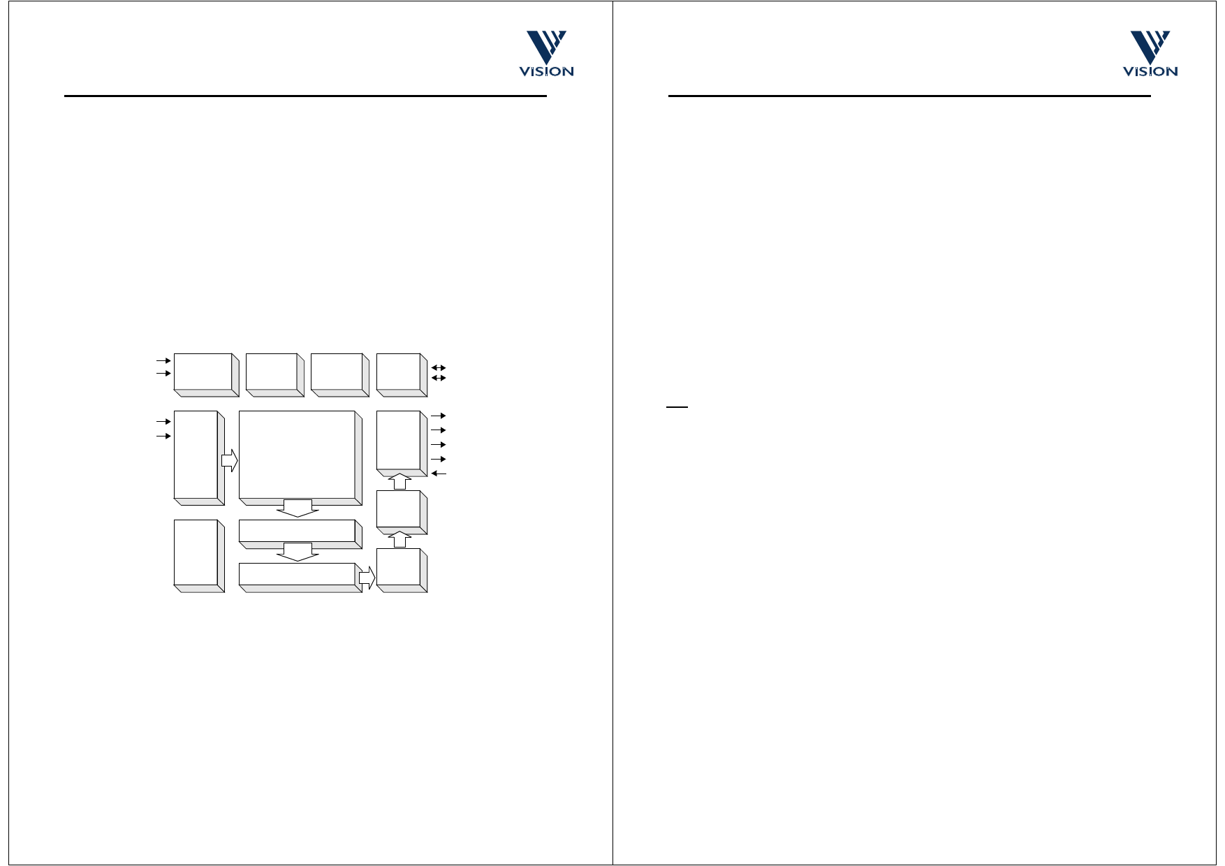
CLKI
MODE
BLACK
CALIBRATION
IMAGE
FORMAT
EXPOSURE
CONTROL
SERIAL
INTER-
FACE
SDA
SCL
RESETB
SIN
VERTICAL
SHIFT
REGISTER
ANALOG
VOLTAGE
REFS.
PHOTO DIODE
ARRAY
SAMPLE & HOLD
HORIZONTAL SHIFT
REGISTER
OUTPUT
FORMAT
8-bit
ADC
D[3:0]
QCK
LST
FST
OEB
GAIN
STAGE
Figure 1.2 : Block Diagram of VV5409 Image Sensor
1.5.1 Digital Data Bus
Along within the pixel-data, codes representing the start and end of fields and the start and end of lines are
embedded within the video-data stream to allow a host controller to synchronise with video-data the camera
module is generating. Section 5. defines the format for the output video-data stream.
The 8-bit data which makes up the video-data stream can be output on the data-bus in one of 3 ways:
1. A series pair of 4-bit nibbles, most significant nibble first, on 4-wires.
2. Four, 2-bit values, most significant 2-bit value first, on 2-wires.
3. Bit-serial data, eight 1-bit values, least significant bit first, on 1-wire.
For the 2, and 1-wire modes, the complement of the data can also be enabled in addition to the data itself.
Commercial In Confidence
cd38041a.fm
08/10/98
5
VV5409 CMOS Monochrome Sensor Datasheet (Restricted) Rev 1.0
1.5.2 Frame Grabber Control Signals
To complement the embedded control sequences, the data qualification clock (QCK), the line-start-signal
(LST) and the field-start-signal (FST), signals can independently be set-up to either be:
1. Disabled
2. Free-running
3. Qualify only the control sequences and the pixel-data
4. Qualify the pixel-data only.
There is also the choice of two different QCK frequencies where one is twice the frequency of the other.
1. Fast QCK: the falling edge of the clock qualifies every 4, 2 or 1-bit block of data that makes up a pixel
value.
2. Slow QCK: the rising edge qualifies the 1st, 3rd, 5th, etc. blocks of data which make up a pixel value,
while the falling edge qualifies the 2nd, 4th, 6th etc. blocks of data. For example, in the 4-wire mode,
the rising edge of the clock qualifies the most significant nibbles, while the falling edge of the clock
qualifies the least significant nibbles.
1.5.3 Synchronisation of Multiple Cameras
Multiple camera configurations can be synchronised by applying a rising edge to the SIN pins once per frame
(every second field).
The FST/DIN pin of the one of cameras (the master) can be re-configured as a SNO output to supply the
synchronidsation signal for the other cameras.
Note: The SNO function has not been verified.
1.5.4 2-wire Serial-Interface
The 2-wire serial-interface provides complete control over how the sensor is setup and run. The sensor serial
address is fixed at 20H.
Two broadcast serial-interface addresses are supported. One allows all sensors to be written to in parallel,
and if a VISION co-processor is in use, the other allows all sensors and co-processors to be written to in
parallel.
Section 6. defines the serial-interface communications protocol, and the register map of all the locations
which can be accessed through the serial-interface.
1.6 System Reset
Using the RESETB pin (active low, internal pull-up), a System Reset of the sensor can be activated. The
sensor behaves exactly as if a power down then power up has taken place, i.e., all sensor serial registers are
reset to their default status, and video timing will be reset.
1.7 Startup configuration of Setup Data
The sensor should be correctly configured on power up, or following a System Reset (Section 1.6), , for
correct operation of the sensor, by writing settings to the camera registers on startup. This applies to the
Setup0 [16], Setup1 [17], and at1 [121] registers in particular.
1.8 Other Features
1.8.1 Microphone Pre-Amplifier
Pins AIN, and AOUT, are the input, and output respectively, for a 2-stage Microphone amplifier. The gain of
this amplifier is programmable through the serial-interface.
The output of the Microphone can be multiplexed at the end of a video line, onto the input of the 8-bit ADC
Commercial In Confidence
cd38041a.fm
08/10/98
6
Share Link: 