IPD090N03LGE8177 View Datasheet(PDF) - Infineon Technologies
Part Name
Description
View to exact match
IPD090N03LGE8177 Datasheet PDF : 9 Pages
| |||
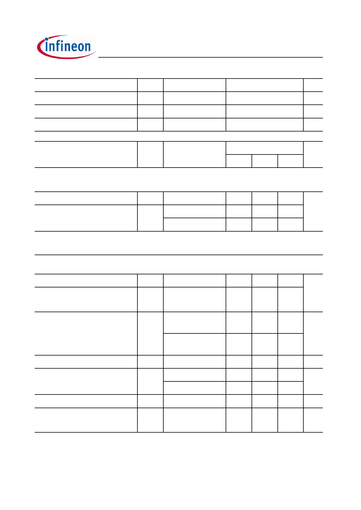
Maximum ratings, at T j=25 °C, unless otherwise specified
Parameter
Symbol Conditions
Power dissipation
P tot
T C=25 °C
Operating and storage temperature T j, T stg
IEC climatic category; DIN IEC 68-1
IPD090N03L G E8177
Value
Unit
42
W
-55 ... 175
°C
55/175/56
Parameter
Symbol Conditions
min.
Values
typ.
Unit
max.
Thermal characteristics
Thermal resistance, junction - case R thJC
-
SMD version, device on PCB
R thJA minimal footprint
-
6 cm² cooling area4)
-
-
3.6 K/W
-
75
-
50
Electrical characteristics, at T j=25 °C, unless otherwise specified
Static characteristics
Drain-source breakdown voltage
V (BR)DSS V GS=0 V, I D=1 mA
30
-
-V
Gate threshold voltage
V GS(th) V DS=V GS, I D=250 µA
1
-
2.2
Zero gate voltage drain current
I DSS
V DS=30 V, V GS=0 V,
T j=25 °C
-
0.1
1 µA
V DS=30 V, V GS=0 V,
T j=125 °C
-
10
100
Gate-source leakage current
Drain-source on-state resistance5)
I GSS
V GS=20 V, V DS=0 V
R DS(on) V GS=4.5 V, I D=30 A
-
10
100 nA
-
10.8 13.5 mW
V GS=10 V, I D=30 A
-
7.5
9
Gate resistance
RG
-
1.1
-W
Transconductance
g fs
|V DS|>2|I D|R DS(on)max,
I D=30 A
26
53
-S
2) See figure 3 for more detailed information
3) See figure 13 for more detailed information
4) Device on 40 mm x 40 mm x 1.5 mm epoxy PCB FR4 with 6 cm2 (one layer, 70 µm thick) copper area for drain
connection. PCB is vertical in still air.
5) Measured from drain tab to source pin
Rev. 2.0
page 2
2014-01-14
Share Link: 