PD45128163G5-A10LI-9JF View Datasheet(PDF) - Elpida Memory, Inc
Part Name
Description
View to exact match
PD45128163G5-A10LI-9JF
Elpida Memory, Inc

PD45128163G5-A10LI-9JF Datasheet PDF : 89 Pages
| |||
µPD45128441-I, 45128841-I, 45128163-I
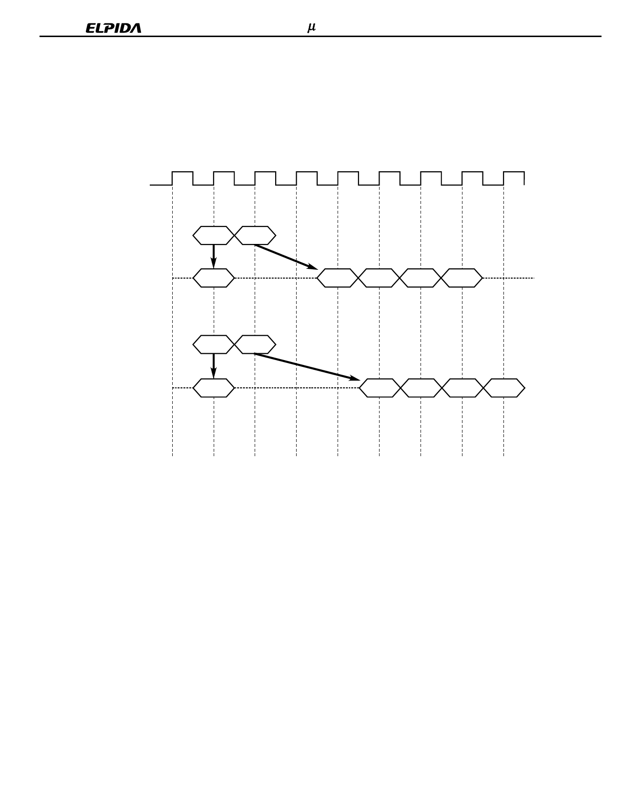
11.3 Write to Read Command Interval
Write command and Read command interval is also 1 cycle.
Only the write data before Read command will be written.
The data bus must be Hi-Z at least one cycle prior to the first DOUT.
Burst length = 4
T0
T1
T2
T3
T4
T5
T6
T7
T8
CLK
/CAS latency = 2
Command
DQ
WRITE A READ B
Hi-Z
DA1
QB1
QB2
QB3
QB4
/CAS latency = 3
Command
DQ
WRITE A READ B
Hi-Z
DA1
QB1
QB2
QB3
QB4
Preliminary Data Sheet E0233N10
29
Share Link: