PD45128163G5-A10LI-9JF View Datasheet(PDF) - Elpida Memory, Inc
Part Name
Description
View to exact match
PD45128163G5-A10LI-9JF
Elpida Memory, Inc

PD45128163G5-A10LI-9JF Datasheet PDF : 89 Pages
| |||
µPD45128441-I, 45128841-I, 45128163-I
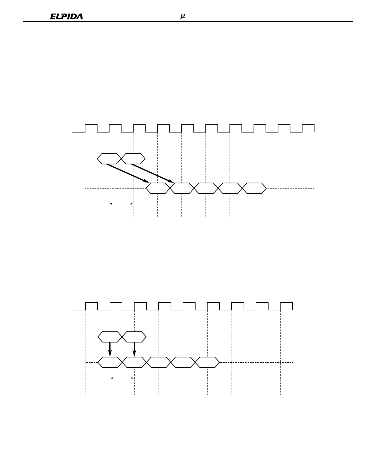
11. Read / Write Command Interval
11.1 Read to Read Command Interval
During a read cycle, when new Read command is issued, it will be effective after /CAS latency, even if the previous
read operation does not completed. READ will be interrupted by another READ.
The interval between the commands is 1 cycle minimum. Each Read command can be issued in every clock
without any restriction.
Burst length = 4, /CAS latency = 2
T0
T1
T2
T3
T4
T5
T6
T7
T8
T9
CLK
Command
READ A READ B
Hi-Z
DQ
QA1
QB1
QB2
QB3
QB4
1cycle
11.2 Write to Write Command Interval
During a write cycle, when a new Write command is issued, the previous burst will terminate and the new burst will
begin with a new Write command. WRITE will be interrupted by another WRITE.
The interval between the commands is minimum 1 cycle. Each Write command can be issued in every clock
without any restriction.
Burst length = 4, /CAS latency = 2
T0
T1
T2
T3
T4
T5
T6
T7
T8
CLK
Command
DQ
WRITE A WRITE B
Hi-Z
DA1
DB1
DB2
DB3
DB4
1cycle
28
Preliminary Data Sheet E0233N10
Share Link: