BSZ123N08NS3G View Datasheet(PDF) - Infineon Technologies
Part Name
Description
View to exact match
BSZ123N08NS3G Datasheet PDF : 9 Pages
| |||
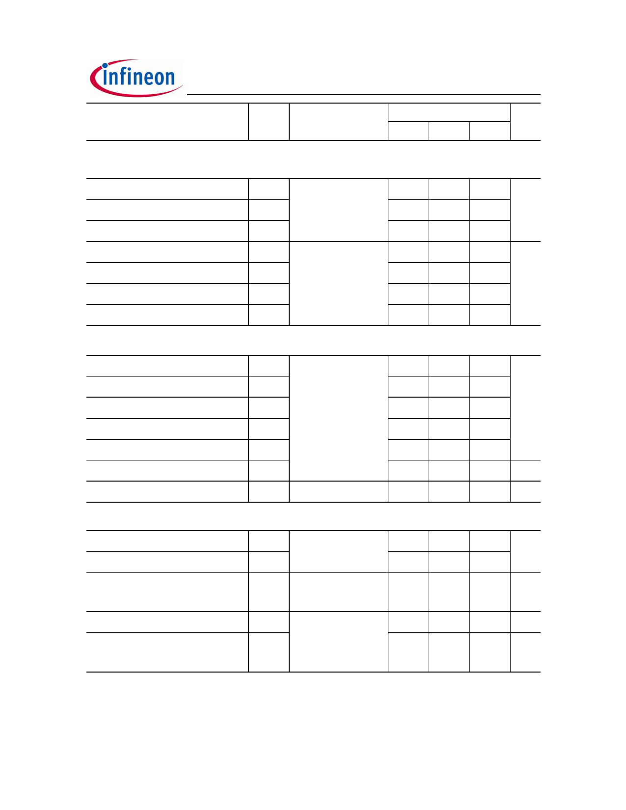
Parameter
Symbol Conditions
BSZ123N08NS3 G
min.
Values
typ.
Unit
max.
Dynamic characteristics
Input capacitance
Output capacitance
Reverse transfer capacitance
Turn-on delay time
Rise time
Turn-off delay time
Fall time
Gate Charge Characteristics5)
Gate to source charge
Gate charge at threshold
Gate to drain charge
Switching charge
Gate charge total
Gate plateau voltage
Output charge
C iss
-
C oss
V GS=0 V, V DS=40 V,
f =1 MHz
-
Crss
-
t d(on)
-
tr
V DD=40 V, V GS=10 V,
-
t d(off)
I D=20 A, R G=1.6 Ω
-
tf
-
Q gs
-
Q g(th)
-
Q gd
V DD=40 V, I D=20 A,
-
Q sw
V GS=0 to 10 V
-
Qg
-
V plateau
-
Q oss
V DD=40 V, V GS=0 V
-
Reverse Diode
Diode continuous forward current I S
-
T C=25 °C
Diode pulse current
I S,pulse
-
Diode forward voltage
V SD
V GS=0 V, I F=20 A,
T j=25 °C
-
Reverse recovery time
Reverse recovery charge
t rr
-
V R=40 V, I F=20A,
Q rr
di F/dt =100 A/µs
-
5) See figure 16 for gate charge parameter definition
1300
350
15
12
18
19
4
1700 pF
470
-
- ns
-
-
-
6.3
- nC
3.6
-
3.8
-
6.5
-
19
25
4.9
-V
25
34
-
40 A
-
160
1.0
1.2 V
45
- ns
54
- nC
Rev. 2.4
page 3
2009-11-12
Share Link: 