BSC072N03LDG View Datasheet(PDF) - Infineon Technologies
Part Name
Description
View to exact match
BSC072N03LDG Datasheet PDF : 10 Pages
| |||
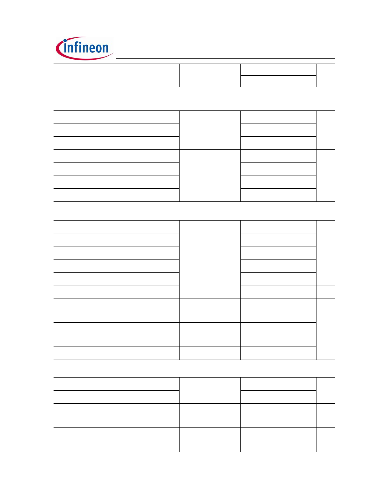
Parameter
Symbol Conditions
BSC072N03LD G
min.
Values
typ.
Unit
max.
Dynamic characteristics
Input capacitance
Output capacitance
Reverse transfer capacitance
Turn-on delay time
Rise time
Turn-off delay time
Fall time
C iss
-
C oss
V GS=0 V, V DS=15 V,
f =1 MHz
-
Crss
-
t d(on)
-
tr
V DD=15 V, V GS=10 V,
-
t d(off)
I D=20 A, R G=1.6 Ω
-
tf
-
Gate Charge Characteristics4)
Gate to source charge
Gate charge at threshold
Gate to drain charge
Switching charge
Gate charge total
Gate plateau voltage
Gate charge total
Gate charge total, sync. FET
Output charge
Q gs
-
Q g(th)
-
Q gd
V DD=15 V, I D=20 A,
-
Q sw
V GS=0 to 4.5 V
-
Qg
-
V plateau
-
Qg
V DD=15 V, I D=20 A,
V GS=0 to 10 V
-
Q g(sync)
V DS=0.1 V,
V GS=0 to 4.5 V
-
Q oss
V DD=15 V, V GS=0 V
-
Reverse Diode
Diode continuous forward current I S
-
T C=25 °C
Diode pulse current
I S,pulse
-
Diode forward voltage
V SD
V GS=0 V, I F=20 A,
T j=25 °C
-
Reverse recovery charge
Q rr
V R=15 V, I F=I S,
di F/dt =400 A/µs
-
4) See figure 16 for gate charge parameter definition
Rev. 1.4
page 3
2600
920
49
6.0
4.0
25
4.0
3500 pF
1200
-
- ns
-
-
-
7.2
- nC
3.8
-
3.4
-
6.8
-
15
20
3.0
-V
31
41
13
- nC
24
-
-
20 A
-
80
0.87
1.1 V
-
10 nC
2009-10-23
Share Link: 