BSC072N03LDG View Datasheet(PDF) - Infineon Technologies
Part Name
Description
View to exact match
BSC072N03LDG Datasheet PDF : 10 Pages
| |||
BSC072N03LD G
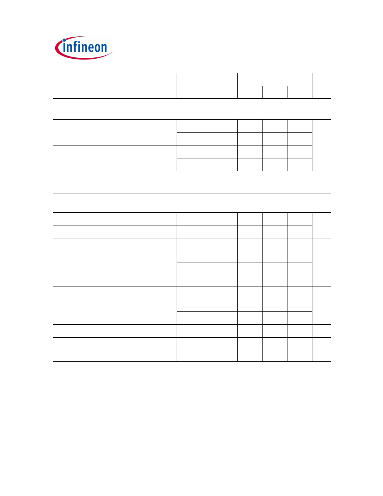
Parameter
Symbol Conditions
Thermal characteristics
Thermal resistance, junction - case R thJC
Thermal resistance, junction -
ambient, 6 cm² cooling area3)
R thJA
bottom
top
t≤10 s
steady state
min.
Values
typ.
Unit
max.
-
-
2.2 K/W
20
-
-
35
-
-
85
Electrical characteristics, at T j=25 °C, unless otherwise specified
Static characteristics
Drain-source breakdown voltage
V (BR)DSS V GS=0 V, I D=1 mA
30
-
-V
Gate threshold voltage
V GS(th) V DS=V GS, I D=250 µA
1
-
2.2
Zero gate voltage drain current
I DSS
V DS=30 V, V GS=0 V,
T j=25 °C
-
0.1
1 µA
Gate-source leakage current
Drain-source on-state resistance
Gate resistance
Transconductance
V DS=30 V, V GS=0 V,
T j=125 °C
-
I GSS
V GS=20 V, V DS=0 V
-
R DS(on) V GS=4.5 V, I D=20 A
-
V GS=10 V, I D=20 A
-
RG
-
g fs
|V DS|>2|I D|R DS(on)max,
I D=20 A
28
10
100
10
100 nA
7.5
9.4 mΩ
6.0
7.2
1.5
2.3 Ω
57
-S
2) See figure 3
3) Device on 40 mm x 40 mm x 1.5 mm epoxy PCB FR4 with 6 cm² (one layer, 70 µm thick) copper area for drain
connection. PCB is vertical in still air. One transistor active.
Rev. 1.4
page 2
2009-10-23
Share Link: 