MJE18002G View Datasheet(PDF) - ON Semiconductor
Part Name
Description
View to exact match
MJE18002G Datasheet PDF : 8 Pages
| |||
MJE18002
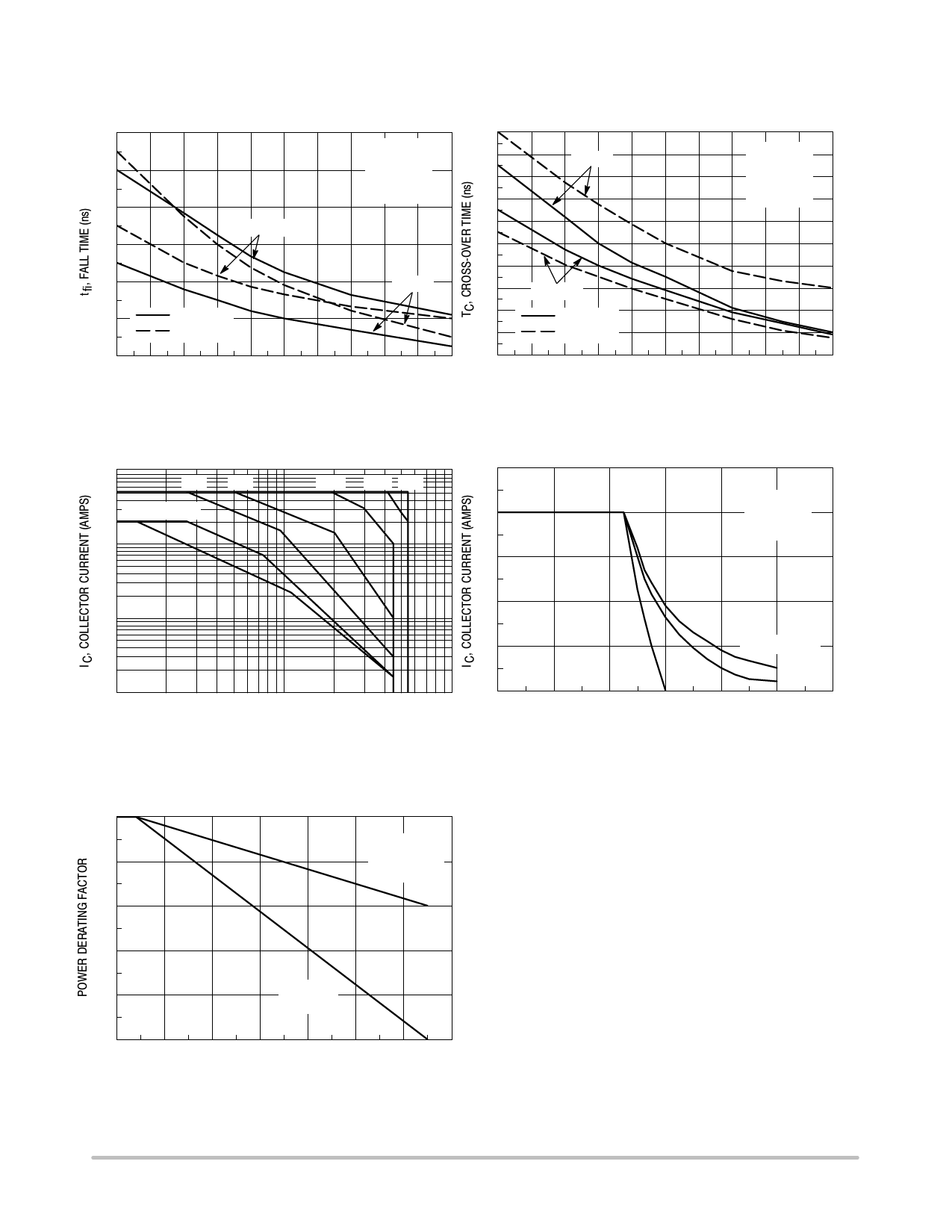
TYPICAL SWITCHING CHARACTERISTICS
(IB2 = IC/2 for all switching)
180
250
160
IB(off) = IC/2
230
VCC = 15 V
VZ = 300 V
210
IC = 1 A
140
LC = 200 mH
190
IC = 0.4 A
170
120
150
IB(off) = IC/2
VCC = 15 V
VZ = 300 V
LC = 200 mH
100
80
TJ = 25°C
TJ = 125°C
IC = 1 A
130
110
IC = 0.4 A
90
TJ = 25°C
70
TJ = 125°C
60
50
55 66 77 88 99 1100 1111 1122 1133 1144 1155
55 6 77 8 9 10 111 12 13 14 1155
hFE, FORCED GAIN
hFE, FORCED GAIN
Figure 13. Inductive Fall Time
Figure 14. Inductive Crossover Time
10.00
5 ms
DC (MJE18002)
1.00
GUARANTEED SAFE OPERATING AREA INFORMATION
2.5
1 ms
50 ms 10 ms 1 ms
2.0
1.5
TC ≤ 125°C
IC/IB ≥ 4
LC = 500 mH
1.0
0.10
0.01
1100
110000
11000000
VCE, COLLECTOR−EMITTER VOLTAGE (VOLTS)
Figure 15. Forward Bias Safe Operating Area
0.5
VBE(off) = 0.5 V
0V
−1.5 V
0.0
0
200
400
600
880000
1000 12102000
VCE, COLLECTOR−EMITTER VOLTAGE (VOLTS)
Figure 16. Reverse Bias Switching Safe Operating Area
There are two limitations on the power handling ability of a
transistor: average junction temperature and second breakdown.
1.0
Safe operating area curves indicate IC−VCE limits of the transistor
SECOND
that must be observed for reliable operation; i.e., the transistor must
0.8
BREAKDOWN
DERATING
not be subjected to greater dissipation than the curves indicate. The
data of Figure 15 is based on TC = 25°C; TJ(pk) is variable
depending on power level. Second breakdown pulse limits are valid
0.6
for duty cycles to 10% but must be derated when TC > 25°C. Second
breakdown limitations do not derate the same as thermal limitations.
Allowable current at the voltages shown on Figure 15 may be found
0.4
at any case temperature by using the appropriate curve on Figure 17.
TJ(pk) may be calculated from the data in Figures 20. At any case
0.2
THERMAL
temperatures, thermal limitations will reduce the power that can be
DERATING
handled to values less the limitations imposed by second
breakdown. For inductive loads, high voltage and current must be
0.0
sustained simultaneously during turn−off with the base to emitter
20
40
60
80
110000 112200 114400
160 junction reverse biased. The safe level is specified as a reverse
TC, CASE TEMPERATURE (°C)
biased safe operating area (Figure 16). This rating is verified under
Figure 17. Forward Bias Power Derating
clamped conditions so that the device is never subjected to an
avalanche mode.
http://onsemi.com
6
Share Link: 