MJE18002G View Datasheet(PDF) - ON Semiconductor
Part Name
Description
View to exact match
MJE18002G Datasheet PDF : 8 Pages
| |||
MJE18002
Preferred Device
SWITCHMODEt
NPN Bipolar Power Transistor
For Switching Power Supply Applications
The MJE18002 have an applications specific state−of−the−art die
designed for use in 220 V line operated Switchmode Power supplies
and electronic light ballasts.
Features
• Improved Efficiency Due to Low Base Drive Requirements:
♦ High and Flat DC Current Gain hFE
♦ Fast Switching
♦ No Coil Required in Base Circuit for Turn−Off (No Current Tail)
• Tight Parametric Distributions are Consistent Lot−to−Lot
• Standard TO−220
• Pb−Free Package is Available*
MAXIMUM RATINGS
Rating
Symbol Value Unit
Collector−Emitter Sustaining Voltage
Collector−Emitter Breakdown Voltage
Emitter−Base Voltage
Collector Current − Continuous
− Peak (Note 1)
Base Current
− Continuous
− Peak (Note 1)
Total Device Dissipation @ TC = 25_C
Derate above 25°C
VCEO
VCES
VEBO
IC
ICM
IB
IBM
PD
450
1000
9.0
2.0
5.0
1.0
2.0
50
0.4
Vdc
Vdc
Vdc
Adc
Adc
W
W/_C
Operating and Storage Temperature
THERMAL CHARACTERISTICS
TJ, Tstg −65 to 150 _C
Characteristics
Symbol
Max
Unit
Thermal Resistance, Junction−to−Case
RqJC
2.5
_C/W
Thermal Resistance, Junction−to−Ambient RqJA
62.5 _C/W
Maximum Lead Temperature for Soldering
TL
Purposes 1/8″ from Case for 5 Seconds
260
_C
Maximum ratings are those values beyond which device damage can occur.
Maximum ratings applied to the device are individual stress limit values (not
normal operating conditions) and are not valid simultaneously. If these limits are
exceeded, device functional operation is not implied, damage may occur and
reliability may be affected.
1. Pulse Test: Pulse Width = 5 ms, Duty Cycle ≤ 10%.
*For additional information on our Pb−Free strategy and soldering details, please
download the ON Semiconductor Soldering and Mounting Techniques
Reference Manual, SOLDERRM/D.
http://onsemi.com
POWER TRANSISTOR
2.0 AMPERES
100 VOLTS − 50 WATTS
1
23
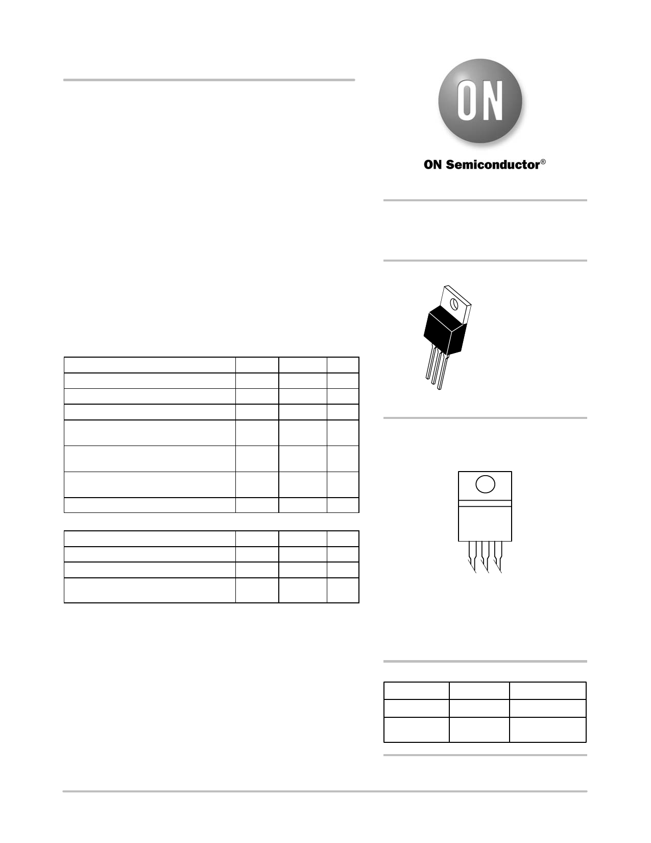
TO−220AB
CASE 221A−09
STYLE 1
MARKING DIAGRAM
MJE18002G
AY WW
A = Assembly Location
Y = Year
WW = Work Week
G = Pb−Free Package
ORDERING INFORMATION
Device
Package
Shipping
MJE18002
TO−220
50 Units / Rail
MJE18002G
TO−220
(Pb−Free)
50 Units / Rail
Preferred devices are recommended choices for future use
and best overall value.
© Semiconductor Components Industries, LLC, 2006
1
February, 2006 − Rev. 6
Publication Order Number:
MJE18002/D
Share Link: 