EDS1232AATA-60TI View Datasheet(PDF) - Elpida Memory, Inc
Part Name
Description
View to exact match
EDS1232AATA-60TI Datasheet PDF : 53 Pages
| |||
EDS1232AATA-TI
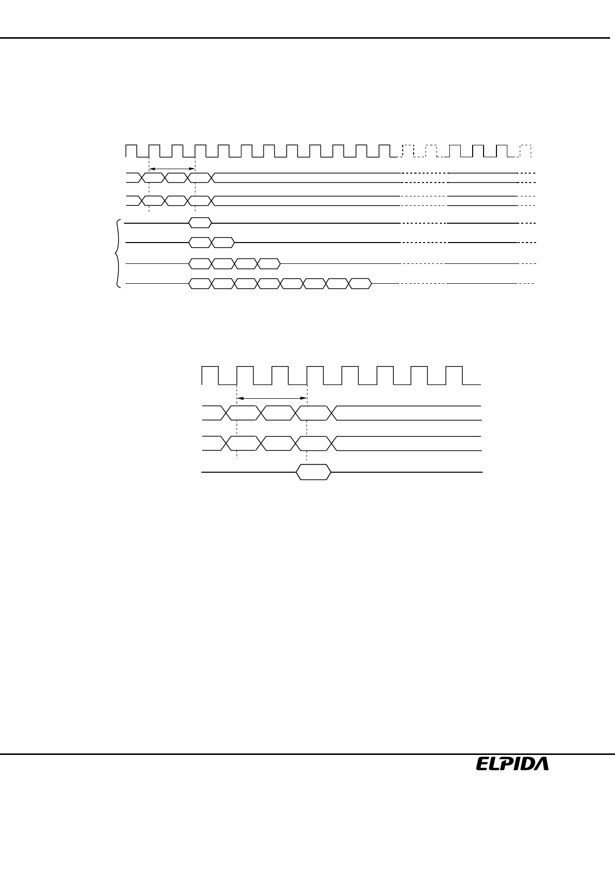
Write operation
Burst write or single write mode is selected by the OPCODE of the mode register.
1. Burst write: A burst write operation is enabled by setting OPCODE (A9, A8) to (0, 0). A burst write starts in the
same clock as a write command set. (The latency of data input is 0 clock.) The burst length can be set to 1, 2, 4
and 8, like burst read operations. The write start address is specified by the column address and the bank select
address at the write command set cycle.
CLK
Command
tRCD
ACT
WRIT
Address
Row
Column
BL = 1
DQ
BL = 2
BL = 4
BL = 8
in 0
in 0 in 1
in 0 in 1 in 2 in 3
in 0 in 1 in 2 in 3 in 4 in 5 in 6 in 7
Burst write
CL = 2, 3
2. Single write: A single write operation is enabled by setting OPCODE (A9, A8) to (1, 0). In a single write
operation, data is only written to the column address and the bank select address specified by the write
command set cycle without regard to the burst length setting. (The latency of data input is 0 clock).
CLK
Command
tRCD
ACT
WRIT
Address
DQ
Row
Column
in 0
Single write
Data Sheet E0305E30 (Ver. 3.0)
28
Share Link: 