EDS1232AATA-75MI View Datasheet(PDF) - Elpida Memory, Inc
Part Name
Description
View to exact match
EDS1232AATA-75MI Datasheet PDF : 53 Pages
| |||
EDS1232AATA-MI
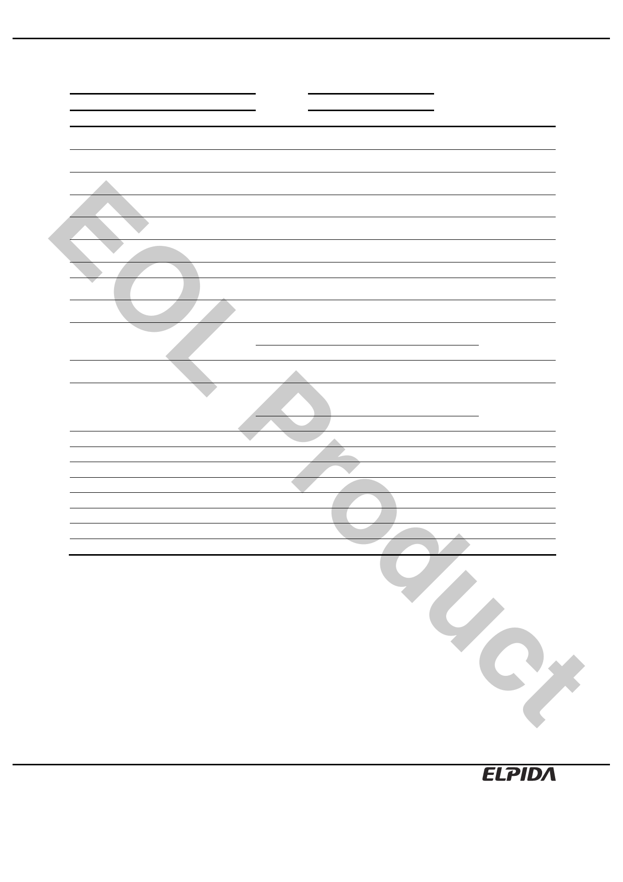
Relationship Between Frequency and Minimum Latency
Parameter
-75
Frequency (MHz)
133
100
tCK (ns)
Symbol
7.5
10
Unit
Notes
Active command to column command
(same bank)
lRCD
3
2
tCK
1
Active command to active command
(same bank)
lRC
9
7
Active command to precharge command
(same bank)
lRAS
6
5
Precharge command to active command
(same bank)
lRP
3
2
Write recovery or data-in to precharge command
E(same bank)
lDPL
2
2
Active command to active command
(different bank)
lRRD
2
2
Self refresh exit time
lSREX
1
1
OLast data in to active command
(Auto precharge, same bank)
lDAL
5
4
Self refresh exit to command input
lSEC
9
7
Precharge command to high impedance
(CL = 2)
lHZP
⎯
2
L (CL = 3)
lHZP
3
3
Last data out to active command
(auto precharge) (same bank)
Last data out to precharge
(early precharge)
(CL = 2)
lAPR
1
1
lEP
⎯
–1
P (CL = 3)
lEP
–2
–2
Column command to column command
lCCD
1
1
Write command to data in latency
lWCD
0
0
DQM to data in
lDID
0
0
r DQM to data out
lDOD
2
2
CKE to CLK disable
lCLE
1
1
o Register set to active command
lMRD
2
2
/CS to command disable
lCDD
0
0
Power down exit to command input
lPEC
1
1
d Notes: 1. lRCD to lRRD are recommended value.
2. Be valid [DESL] or [NOP] at next command of self refresh exit.
uct 3. Except [DESL] and [NOP]
tCK
1
tCK
1
tCK
1
tCK
1
tCK
1
tCK
2
tCK
= [lDPL + lRP]
tCK
= [lRC]
3
tCK
tCK
tCK
tCK
tCK
tCK
tCK
tCK
tCK
tCK
tCK
tCK
tCK
Data Sheet E0340E30 (Ver. 3.0)
8
Share Link: 