EDS1232AATA-75MI View Datasheet(PDF) - Elpida Memory, Inc
Part Name
Description
View to exact match
EDS1232AATA-75MI Datasheet PDF : 53 Pages
| |||
EDS1232AATA-MI
Command Operation
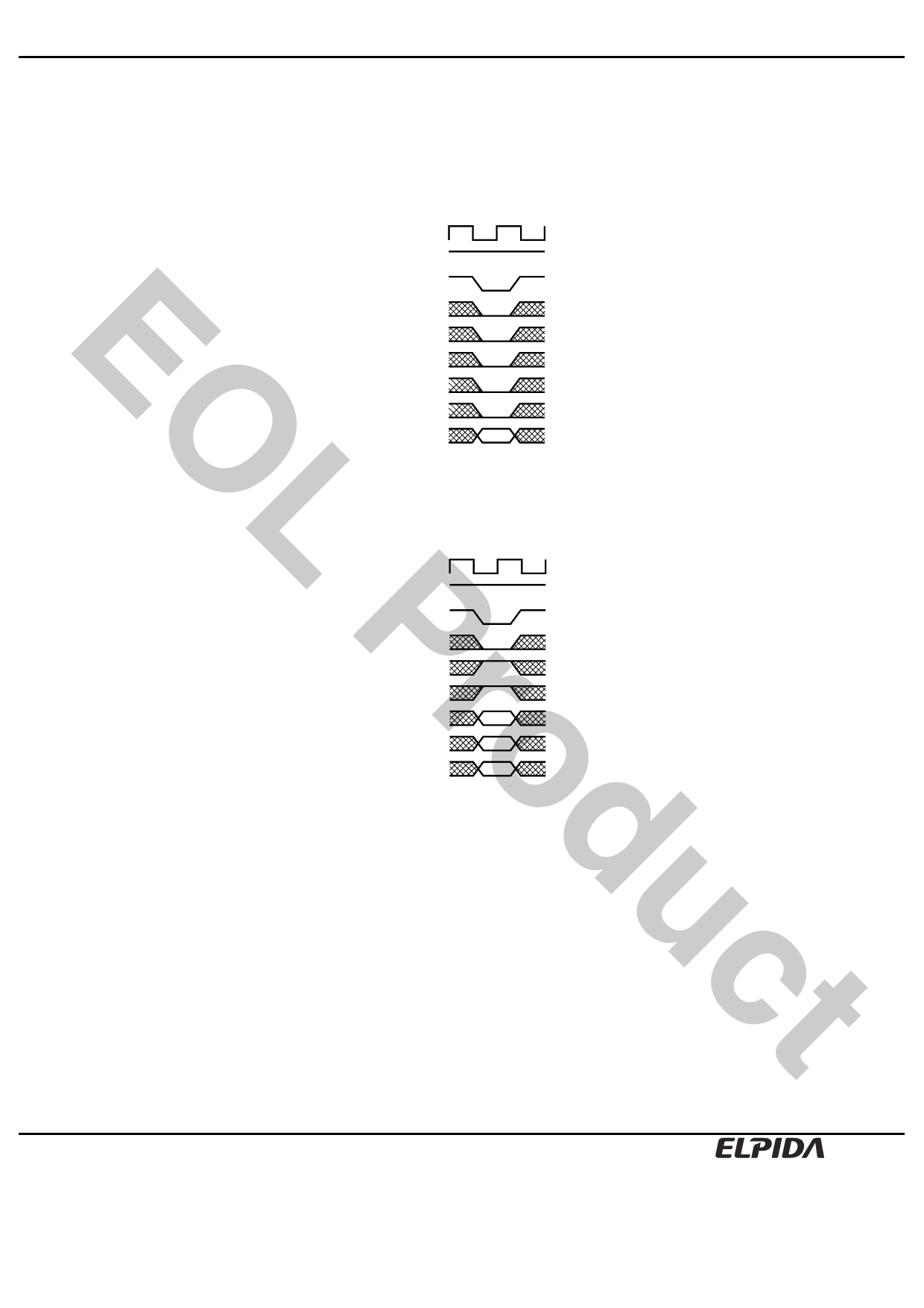
Mode register set command (/CS, /RAS, /CAS, /WE)
The Synchronous DRAM has a mode register that defines how the device operates. In this command, A0 through
A11 are the data input pins. After power on, the mode register set command must be executed to initialize the
device. The mode register can be set only when all banks are in idle state. During 2CLK (tRSC) following this
command, the Synchronous DRAM cannot accept any other commands.
CLK
CKE H
/CS
/RAS
E /CAS
/WE
BA0, BA1
(Bank select)
A10
O Add
Mode Register Set Command
Activate command (/CS, /RAS = Low, /CAS, /WE = High)
The Synchronous DRAM has four banks, each with 4,096 rows. This command activates the bank selected by BA0
L and BA1 and a row address selected by A0 through A11. This command corresponds to a conventional DRAM's
/RAS falling.
CLK
CKE H
P/CS
/RAS
/CAS
/WE
rBA0, BA1
(Bank select)
oA10
Row
Add
Row
duct Row Address Strobe and Bank Activate Command
Data Sheet E0340E30 (Ver. 3.0)
11
Share Link: 