NOIL2SM1300A View Datasheet(PDF) - ON Semiconductor
Part Name
Description
View to exact match
NOIL2SM1300A Datasheet PDF : 44 Pages
| |||
NOIL2SM1300A
SENSOR ARCHITECTURE
Image Sensor Core
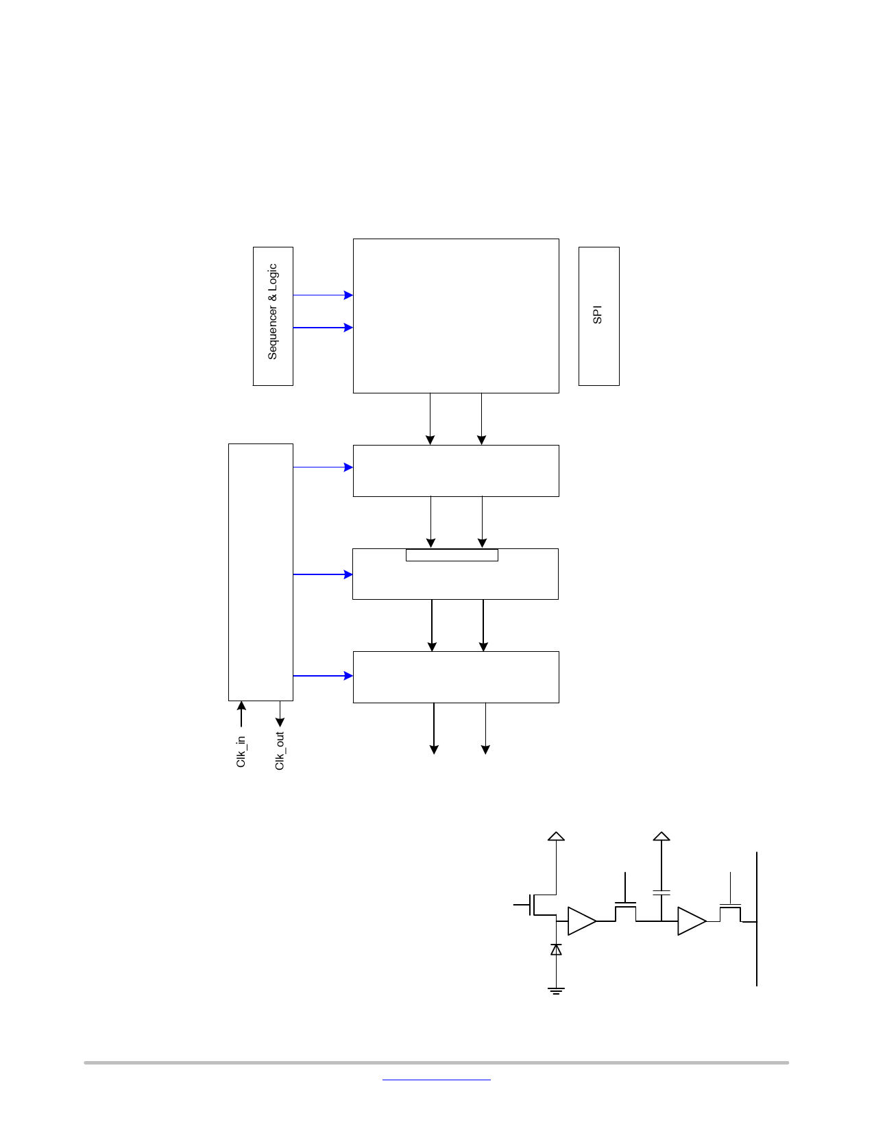
The floor plan of the architecture is shown in Figure 5. The
sensor consists of a pixel array, analog front end, data block,
and LVDS transmitters and receivers. Separate modules for
the SPI, clock division, and sequencer are also integrated.
The image sensor of 1280 x 1024 active pixels is read out in
progressive scan.
This architecture enables programmable addressing in the
x-direction in steps of 24 pixels, and in the y-direction in
steps of one pixel. The starting point of the address can be
uploaded by the SPI.
The AFE prepares the signal for the digital data block
when the data is multiplexed and prepared for the LVDS
interface.
Clk X & Clk Y
Pixel Array
(1280x1024)
31.5 Mhz
Clock
Divider
63 Mhz
28 Analog Channels, 31.5 Msps
Analog Front End (AFE)
24 x 10−bit Digital Channels, 31.5 Msps
Local registers
Data Formatting
12 x 10−bit Digital Channels, 63 Msps
315 Mhz
LVDS Interface Tx and Rx
12 x LVDS Outputs at 630 Msps
Figure 6. Floor Plan of the Sensor
The 6T Pixel
To obtain the global shutter feature combined with a high
sensitivity and good parasitic light sensitivity (PLS),
implement the pixel architecture shown in Figure 6. This
pixel architecture is designed with a 14 mm x 14 mm pixel
pitch to meet the specifications listed in Table 1 and Table 2
on page 3. This architecture also enables pipelined or
triggered mode.
Vpix
Reset
Vmem
Sample
Select
Figure 7. 6T Pixel Architecture
www.onsemi.com
8
Share Link: 