NOIL2SM1300A View Datasheet(PDF) - ON Semiconductor
Part Name
Description
View to exact match
NOIL2SM1300A Datasheet PDF : 44 Pages
| |||
NOIL2SM1300A
Table 6. AC ELECTRICAL CHARACTERISTICS (Note 1)
The following specifications apply for VDD = 2.5 V, Clock = 315 MHz, 500 fps.
Symbol
FCLK
DCCLK
DCD
fps
Parameter
Input Clock Frequency
Clock Duty Cycle
Duty Cycle Distortion
Jitter
Frame Rate
Condition
fps = 500
At maximum clock
At maximum clock
peak-to-peak
Maximum clock speed
Typ
Max Units
315
MHz
50
%
250
ps
50
ps
500
fps
NOTE: Duty Cycle Distortion and Jitter is passed directly from input to output. Therefore, DCD and Jitter tolerance depends on the
customer’s system clock generation circuitry.
OVERVIEW
This data sheet describes the interface of the LUPA1300-2
image sensor. The SXGA resolution CMOS active pixel
sensor features synchronous shutter and a maximal frame
rate of 500 fps in full resolution. The readout speed is
boosted by sub sampling and the windowed region of
interest (ROI) readout. FPN correction cannot be used in
conjunction with sub-sampling and windowed region of
interest readout for windows starting with non zero kernel
address. High dynamic range scenes can be captured using
the double and multiple slope functionality. User
programmable row and column start and stop positions
enables windowing. Sub sampling reduces resolution while
maintaining the constant field of view and an increased
frame rate.
The LUPA1300-2 sensor has 12 LVDS high speed outputs
that transfer image data over longer distances. This
simplifies the surrounding system. The LVDS interface can
receive high speed and wide bandwidth data signals and
maintain low noise and distortion. A special training mode
enables the receiving system to synchronize the incoming
data stream when switching to master, slave, or triggered
mode. The image sensor also integrates a programmable
offset and gain amplifier for each channel.
A 10-bit ADC converts the analog signal to a 10-bit digital
word stream. The sensor uses a 3-wire Serial Peripheral
Interface (SPI). It requires only one master clock for
operation up to 500 fps.
The sensor is available in a monochrome version or Bayer
(RGB) patterned color filter array. It is placed in a 168-pin
ceramic mPGA package.
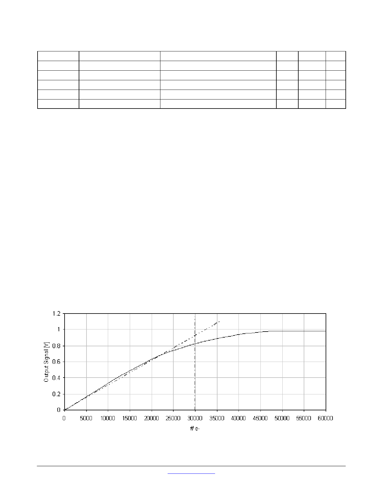
Figure 2 depicts the photovoltaic response of the
LUPA1300−2. Figure 3 shows the spectral response for the
mono and color versions of LUPA1300-2.
Photovoltaic Response Curve
Figure 3. Photovoltaic Response of LUPA1300−2
www.onsemi.com
6
Share Link: 