VP5511B View Datasheet(PDF) - Zarlink Semiconductor Inc
Part Name
Description
View to exact match
VP5511B Datasheet PDF : 17 Pages
| |||
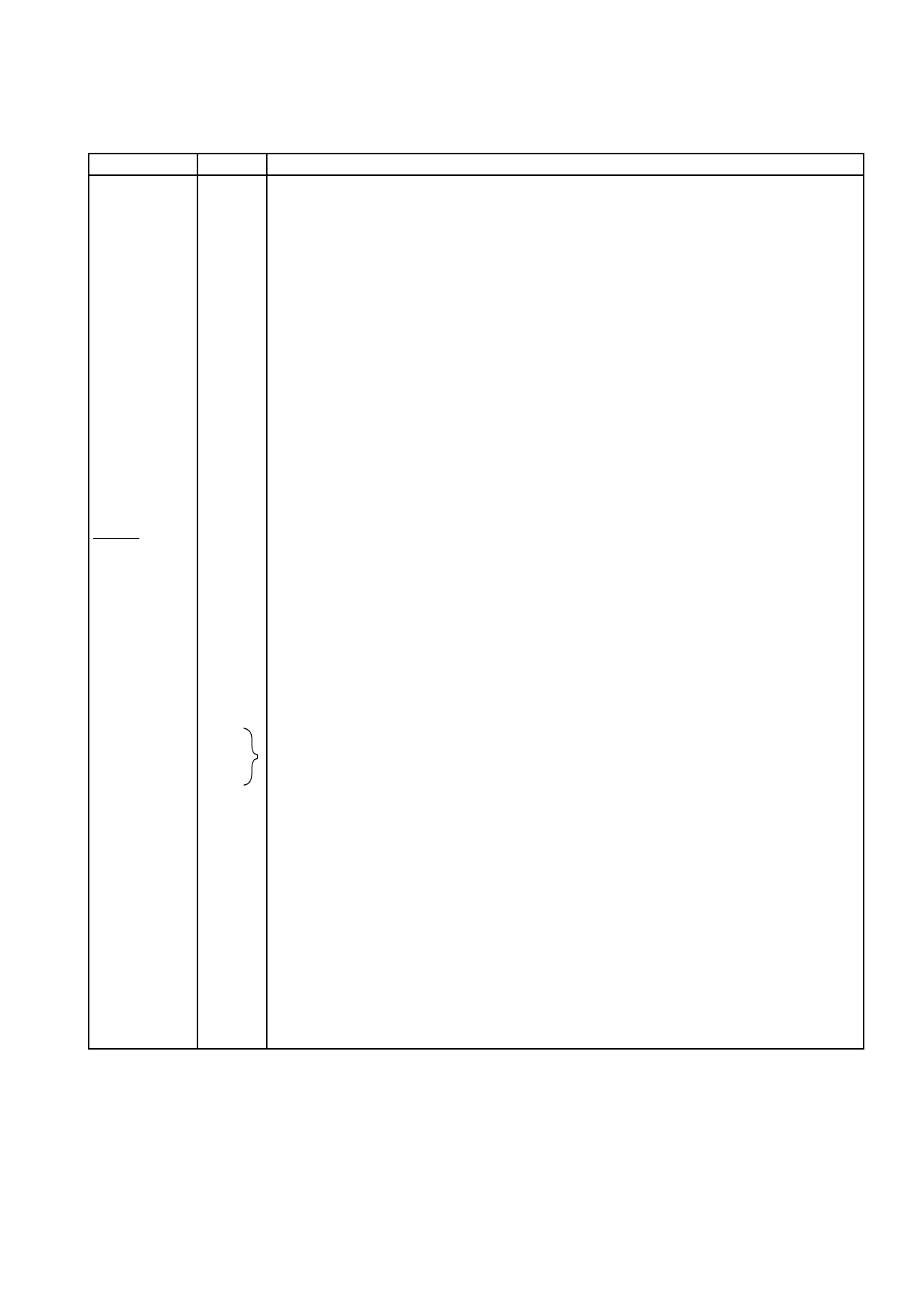
VP5311B/VP5511B
PIN DESCRIPTIONS
Pin Name
PD0-7
D0-7
PXCK
CLAMP
COMPSYNC
TDO
TDI
TMS
TCK
SA1
SA2
SCL
SDA
RESET
REFSQ
VREF
DAC GAIN
COMP
LUMAOUT
COMPOUT
CHROMAOUT
NOT USED
VDD
AVDD
GND
AGND
Pin No.
39 - 46
3 - 10
15
17
18
21
22
23
24
26
27
28
30
34
35
50
51
52
54
56
58
60, 61, 64
1, 12, 16,
20, 29,
32, 33,
37, 48
53, 59
62, 63
2, 11, 13,
14, 19,
25, 31,
36, 38, 47
49, 55, 57
Description
8 Bit Pixel Data inputs clocked by PXCK. PD0 is the least significant bit, corresponding to Pin
46. These pins are internally pulled low.
8 Bit General Purpose Port input/output. D0 is the least significant bit, corresponding to Pin 3.
These pins are internally pulled low.
27MHz Pixel Clock input. The VP5311 internally divides PXCK by two to provide the pixel
clock.
The CLAMP output signal is synchronised to COMPSYNC output and indicates the position of
the BURST pulse, (lines 10-263 and 273-525 for NTSC; lines 6-310 and 319-623 for PAL-
B,D, G,I,N(Argentina)).
Composite sync pulse output. This is an active low output signal.
JTAG Data scan output port.
JTAG Data scan input port.
JTAG Scan select input.
JTAG Scan clock input.
Slave address select.
Slave address select.
Standard I2C bus serial clock input.
Standard I2C bus serial data input/output.
Master reset. This is an asynchronous, active low, input signal and must be asserted for a
minimum 200ns in order to reset the VP5311.
Reference square wave input used only during Genlock mode.
Voltage reference output. This output is nominally 1·055V and should be decoupled with a
100nF capacitor to GND.
DAC full scale current control. A resistor connected between this pin and GND sets the
magnitude of the video output current. An internal loop amplifier controls a reference current
flowing through this resistor so that the voltage across it is equal to the Vref voltage.
DAC compensation. A 100nF ceramic capacitor must be connected between pin 52 and pin
53.
True luminance, composite and chrominance video signal outputs. These are high
impedance current source outputs. A DC path to GND must exist from each of these pins.
Positive supply input. All VDD pins must be connected.
Analog positive supply input. All AVDD pins must be connected.
Negative supply input. All GND pins must be connected.
Negative supply input. All AGND pins must be connected.
All other pins are N/C and should not be connected.
5
Share Link: 