VP5511B View Datasheet(PDF) - Zarlink Semiconductor Inc
Part Name
Description
View to exact match
VP5511B Datasheet PDF : 17 Pages
| |||
VP5311B/VP5511B
SDA
SCL
SA1
SA2
I2C INTERFACE
SET-UP
REGISTERS
ANTI-TAPING
CONTROL
CLOSED
CAPTION
CLAMP
RESET
VIDEO TIMING GENERATOR
+
COMPSYNC
SYNC
BLANK
+
Y
INTERPOLATOR
INSERT
INPUT
DEMUX
8
&
PD7-0 CHROMA
INTERP
Cr
CHROMA
LOW -PASS
INT ER POLATOR
MODULATOR
FILTER
Cb
PXCK
LUMA OUT
LUMA
DAC
+
COMP
COMP
DAC
OUT
CHROMA
DAC
CHROMA OUT
8
D7-0
GENERAL
PURPOSE PORT
DIGITAL
PHASE COMP
REFSQ
COLOUR SUBCARRIER
GENERATOR
JTAG.
TDO
TDI
TMS TCK
DAC
REF
DACGAIN
VREF
COMP
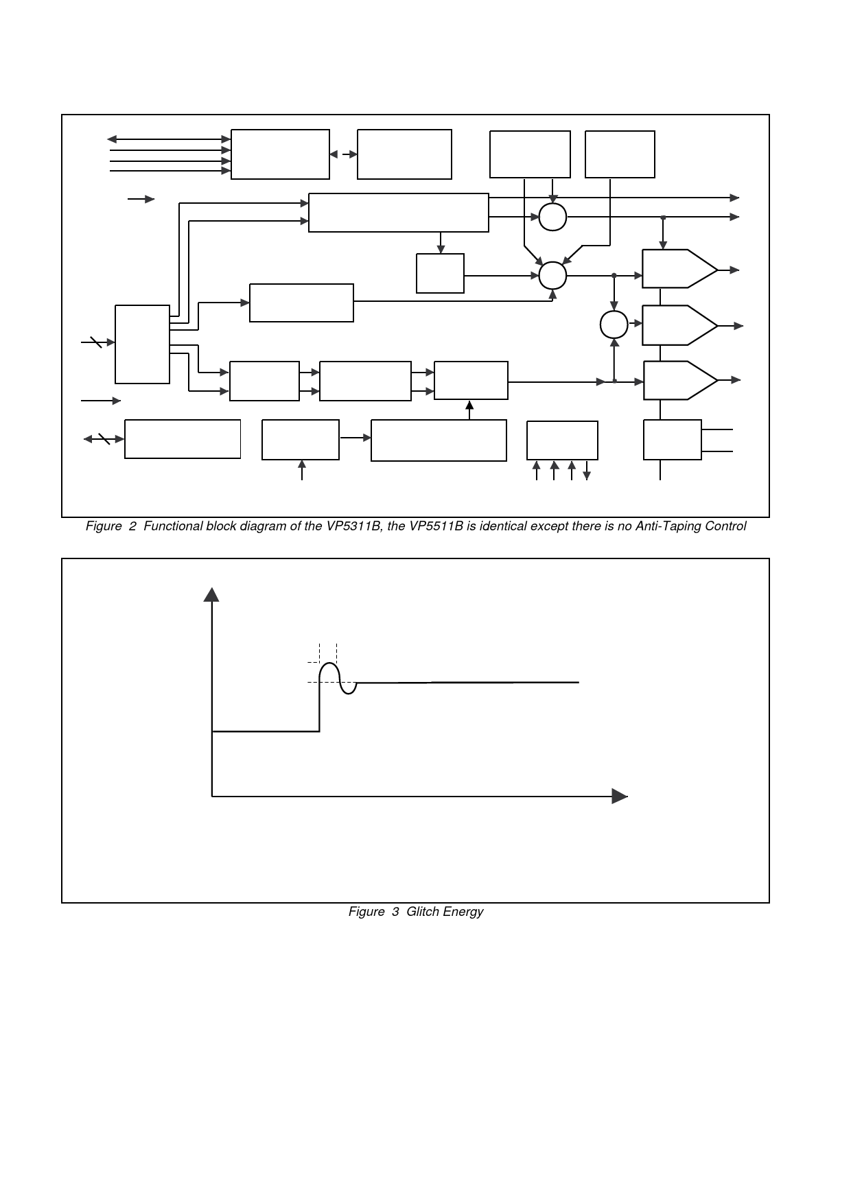
Figure 2 Functional block diagram of the VP5311B, the VP5511B is identical except there is no Anti-Taping Control
V
W
H
Peak Glitch Area = H x W/2
The glitch energy is calculated by measuring the area under the voltage
time curve for any LSB step, typically specified in picoVolt-seconds (pV-s)
t(ps)
Figure 3 Glitch Energy
4
Share Link: 