VP5511B View Datasheet(PDF) - Zarlink Semiconductor Inc
Part Name
Description
View to exact match
VP5511B Datasheet PDF : 17 Pages
| |||
VP5311B/VP5511B
this sets registers as follows:
reg
04
fb
ff
data
08
0b
01
Note: HSOFF should always be zero when using slave mode.
Video Timing - Master sync mode
When TRSEL (bit 0 of GPSCTL register) is set high, the
VP5311 operates in a MASTER sync mode, all REC656
timing reference codes are ignored and GPP bits D0 - 4
become a video timing port with VS, HS and FIELD outputs.
The PXCK signal is, however, still used to generate all internal
clocks. When TRSEL is set high, the direction setting of bits 4
- 0 of the GPPCTL register is ignored.
VS is the start of the field sync datum in the middle of the
equalisation pulses. HS is the line sync which is used by the
preceding MPEG2 decoder to define when to output digital
video data to the VP5311. The position of the falling edge of
HS relative to the first data Cb0, can be programmed in
HSOFFM-L registers, see fig. 4.
HS offset
The position of the falling edge of HS relative to the first
data Cb0, can be programmed in HSOFFM-L registers, see
figure 4, this is called the pipeline delay and may need
adjusting for a particular application. This is done by
programming a 10 bit number called HSOFF into the
HSOFFM and HSOFFL registers, HSOFFM being the most
significant two bits and HSOFFL the least significant eight bits.
A default value of 07EH is held in the registers.
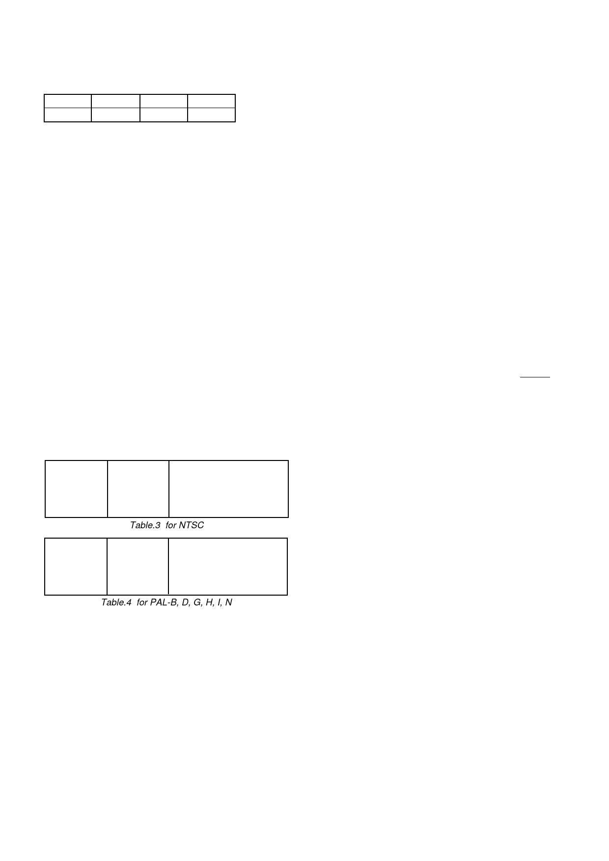
The value to program into HSOFF can be looked up in
tables 3 &4:
NCK
0 to 120
121 to 138
184 to 857
HSOFF
Comment
126 to 6
HS normal (64 cks)
863 to 801
HS pulse shortened*
800 to 127
HS normal (64 cks)
Table.3 for NTSC
NCK
HSOFF
Comment
0 to 131
137 to 6
HS normal (64 cks)
132 to 194 869 to 807
HS pulse shortened*
195 to 863 806 to 138
HS normal (64 cks)
Table.4 for PAL-B, D, G, H, I, N
where NCK = number of 13.5MHz clock cycles between the
falling edge of HS and Cb0 (first data I/P on PD7-0) see fig. 4.
Decreasing HSOFF advances the HS pulse (numbers are in
decimal).
*HS pulse shortened means that the width of the pulse will be
less than the normal 64 13.5MHz clock cycles.
The interruption in the sequence of values is because the HS
signal is jumping across a line boundary to the previous line as
the offset is increased. The register default value is 7EH and
this sets Nck to 0, ie. the HS negative edge and Cb0 are co-
incident in NTSC mode.
Genlock using REFSQ input
The VP5311 can be Genlocked to another video source by
setting GENLKEN high (in GPSCTL register) and feeding a
phase coherent sub carrier frequency signal into REFSQ.
Under normal circumstances, REFSQ will be the same
frequency as the sub carrier. But by setting FSC4SEL high (in
GPSCTL register), a 4 x sub carrier frequency signal may be
input to REFSQ. In this case, the Genlock circuit can be reset
to the required phase of REFSQ, by supplying a pulse to
SCSYNC (pin 9). The frequency of SCSYNC can be at sub
carrier frequency, but once per line, or once per field could be
adequate, depending on the application. When GENLKEN is
set high, the direction setting of bit 6 in the GPPCTL register
is igonred.
PALID Input
When in Genlock mode with GENLKEN set high (in
GPSCTL register), the VP5311 requires a PAL phase
identification signal, to define the correct phase on every line.
This is supplied to PALID input (pin 10), High = -135° and low
= +135°. The signal is asynchronous and should be changed
before the sub carrier burst signal. PALID input is enabled by
setting PALIDEN high (in GPSCTL register). When
GENLKEN is high, the direction setting of bit 7 of the GPPCTL
register is ignored
Master Reset
The VP5311/VP5511 must be initialised with the RESET
pin 34. This is an asynchronous active low signal and must be
active for a minimum of 200ns in order for the VP5311/
VP5511 to be reset. The device resets to line 64, start of
horizontal sync (i.e. line blanking active). There is no on-chip
power on reset circuitry.
Line 21 coding
Two bytes of data are coded on the line 21 of each field,
see figure 7. In the NTSC Closed Caption service, the default
state is to code on line 21 of field one only. An additional
service can also be provided using line 21 (284) of the second
field. The data is coded as NRZ with odd parity, after a clock
run-in and framing code. The clock run-in frequency =
0.5034965MHz which is related to the nominal line period, D
= H / 32.
D = 63.55555556 / 32µs
Two data bytes per field are loaded via I2C bus registers
CCREG1-4. Each field can be independently enabled by
programming the enable bits in the control register (CC_CTL).
The data is cleared to zero in the Closed Caption shift
registers after it has been encoded by the VP5311/VP5511.
Two status bit are provided (in CC_CTL), which are set high
when data is written to the registers and set low when the data
has been encoded on the Luma signal. The data is cleared to
zero in the Closed Caption shift registers after it has been
encoded by the VP5311/VP5511. The next data bytes must
be written to the registers when the status bit goes high,
otherwise the Closed Caption data output will contain Null
characters. If a transmission slot is missed (ie. no data
received) the encoder will send Null characters. Null
characters are invisible to a closed caption reciever. The MSB
(bit 7) is the parity bit and is automatically added by the
encoder.
10
Share Link: 