BSB013NE2LXI View Datasheet(PDF) - Infineon Technologies
Part Name
Description
View to exact match
BSB013NE2LXI Datasheet PDF : 11 Pages
| |||
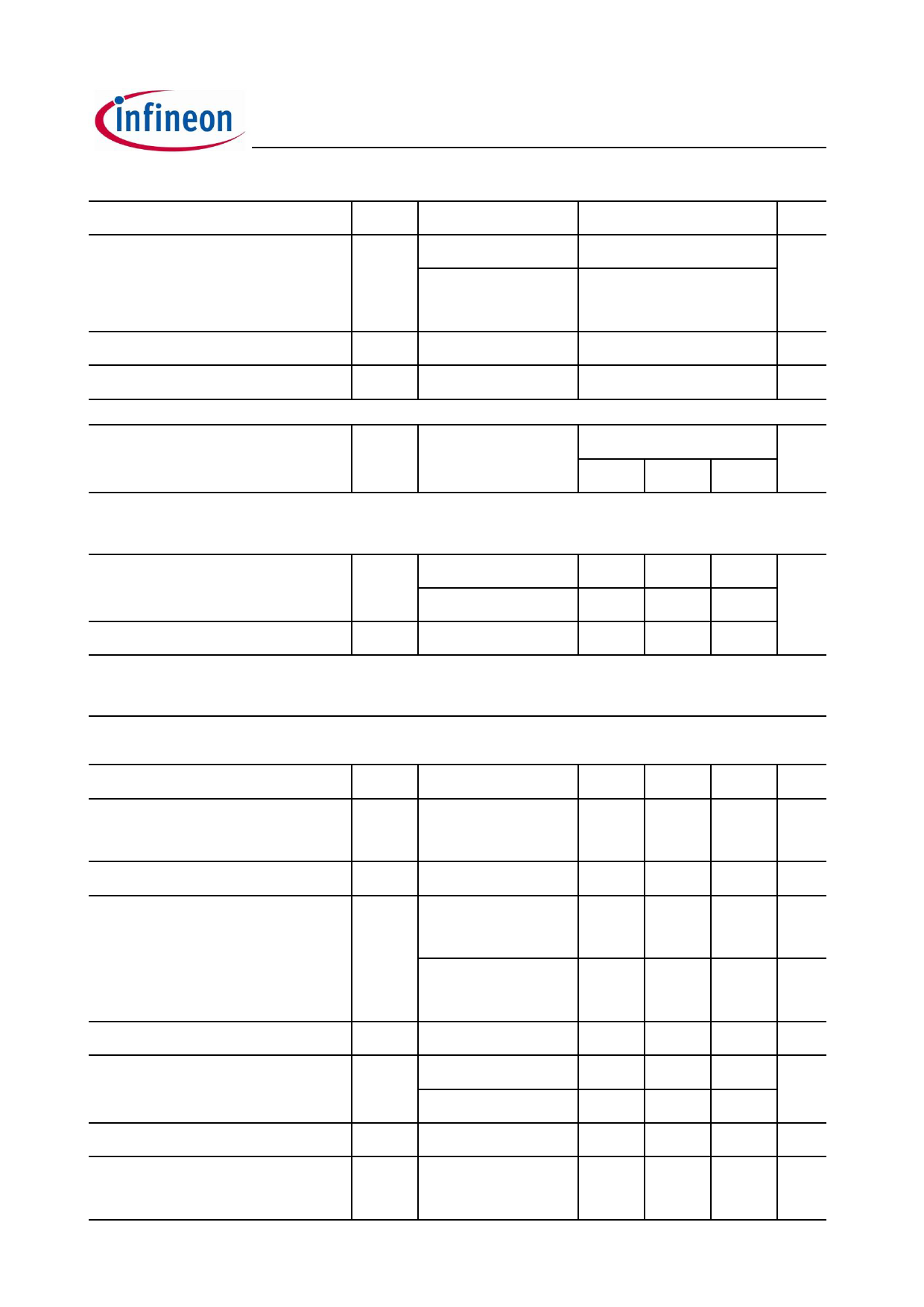
Maximum ratings, at T j=25 °C, unless otherwise specified
Parameter
Symbol Conditions
Power dissipation
P tot
T C=25 °C
T A=25 °C,
R thJA=45 K/W
Operating and storage temperature T j, T stg
IEC climatic category; DIN IEC 68-1
BSB013NE2LXI
Value
Unit
57
W
2.8
-40 … 150
°C
Parameter
Symbol Conditions
min.
Values
typ.
Unit
max.
Thermal characteristics
Thermal resistance, junction - case R thJC bottom
-
1.0
- K/W
top
-
-
2.2
Device on PCB
R thJA 6 cm2 cooling area3)
-
-
45
Electrical characteristics, at T j=25 °C, unless otherwise specified
Static characteristics
Drain-source breakdown voltage
V (BR)DSS V GS=0 V, I D=10 mA
25
-
-V
Breakdown
voltage
temperature
coefficd/dieVTn(Bjt R)DSS
I D=10 mA,
to 25 °C
referenced
-
15
- mV/K
Gate threshold voltage
V GS(th) V DS=V GS, I D=250 µA
1.2
-
2V
Zero gate voltage drain current
I DSS
V DS=20 V, V GS=0 V,
T j=25 °C
-
25
500 µA
V DS=20 V, V GS=0 V,
T j=125 °C
-
4
- mA
Gate-source leakage current
I GSS
V GS=20 V, V DS=0 V
-
10
100 nA
Drain-source on-state resistance
R DS(on) V GS=4.5 V, I D=30 A
-
1.4
1.8 mW
V GS=10 V, I D=30 A
-
1.1
1.3
Gate resistance
RG
0.3
0.6
1.2 W
Transconductance
g fs
|V DS|>2|I D|R DS(on)max,
I D=30 A
85
170
-S
Rev. 2.4
page 2
2013-02-12
Share Link: 