M27C2001-70F1(1995) View Datasheet(PDF) - STMicroelectronics
Part Name
Description
View to exact match
M27C2001-70F1 Datasheet PDF : 14 Pages
| |||
M27C2001
AC MEASUREMENT CONDITIONS
Input Rise and Fall Times
Input Pulse Voltages
Input and Output Timing Ref. Voltages
≤ 20ns
0.4V to 2.4V
0.8V to 2.0V
Note that Output Hi-Z is defined as the point where data
is no longer driven.
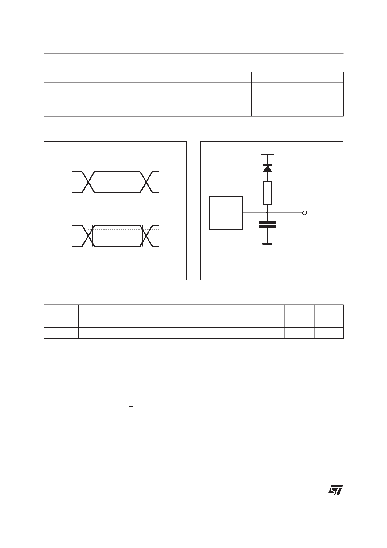
Figure 3. AC Testing Input Output Waveforms
2.4V
0.4V
2.0V
0.8V
AI00826
Figure 4. AC Testing Load Circuit
1.3V
1N914
DEVICE
UNDER
TEST
3.3kΩ
OUT
CL = 100pF
CL includes JIG capacitance
AI00828
Table 5. Capacitance (1) (TA = 25 °C, f = 1 MHz )
Symbol
Parameter
CIN
Input Capacitance
COUT
Output Capacitance
Note: 1. Sampled only, not 100% tested.
Test Condition
Min
VIN = 0V
VOUT = 0V
Max
6
12
Unit
pF
pF
Table 6. Read Mode DC Characteristics (1)
(TA = 0 to 70 °C or –40 to 85 °C; VCC = 5V ± 5% or 5V ± 10%; VPP = VCC)
Symbol
Parameter
Test Condition
Min
ILI
Input Leakage Current
0V ≤ VIN ≤ VCC
ILO
Output Leakage Current
0V ≤ VOUT ≤ VCC
ICC
Supply Current
E = VIL, G = VIL,
IOUT = 0mA, f = 5MHz
ICC1 Supply Current (Standby) TTL
E = VIH
ICC2 Supply Current (Standby) CMOS
E > VCC – 0.2V
IPP
Program Current
VPP = VCC
VIL
VIH (2)
Input Low Voltage
Input High Voltage
–0.3
2
VOL Output Low Voltage
IOL = 2.1mA
Output High Voltage TTL
VOH
Output High Voltage CMOS
IOH = –400µA
IOH = –100µA
2.4
VCC – 0.7V
Notes: 1. VCC must be applied simultaneously with or before VPP and removed simultaneously or after VPP.
2. Maximum DC voltage on Output is VCC +0.5V.
Max
±10
±10
30
1
100
10
0.8
VCC + 1
0.4
Unit
µA
µA
mA
mA
µA
µA
V
V
V
V
V
4/14
Share Link: 