VP551E View Datasheet(PDF) - Mitel Networks
Part Name
Description
View to exact match
VP551E Datasheet PDF : 16 Pages
| |||
VP531E/VP551E
represents one 13.5MHz cycle. To calculate this use the
formula below:
NTSC/PALM
HCNT = SN + 119 (SN = 0 - 738)
HCNT = SN + 739 (SN = 739 - 857)
PAL
HCNT = SN + 127 (SN = 0 - 738)
HCNT = SN + 737 (SN = 737 - 863)
where SN is Rec. 656/601 sample number on which the
negative edge of HSYNC occurs.
SL_HS
A further adjustment is also required to ensure that the
correct Cr and Cb sample alignment. The bits SL_HS1-0
allows for four sampling positions in the CbYCrY sequence,
failure to set this correctly will mean corruption of the colour or
colour being interpreted as luma.
F_SWAP
If the field synchronisation is wrong it can be swapped by
setting this bit.
V_SYNC
When set to a '1' this bit allows an odd/even square wave
to provide the field synchronisation.
Video Timing - Master sync mode
When TRSEL (bit 0 of GPSCTL register) is set high, the
VP531 operates in a MASTER sync mode, all REC656 timing
reference codes are ignored and GPP bits D0 - 4 become a
video timing port with VS, HS and FIELD outputs. The PXCK
signal is, however, still used to generate all internal clocks.
When TRSEL is set high, the direction setting of bits 4 - 0 of
the GPPCTL register is ignored.
VS is the start of the field sync datum in the middle of the
equalisation pulses. HS is the line sync which is used by the
preceding MPEG2 decoder to define when to output digital
video data to the VP531. The position of the falling edge of HS
relative to the first data Cb0, can be programmed in HSOFFM-
L registers.
HS offset
The position of the falling edge of HS relative to the first
data Cb0, can be programmed in HSOFFM-L registers, see
figure 4, this is called the pipeline delay and may need
adjusting for a particular application. This is done by
programming a 10 bit number called HSOFF into the
HSOFFM and HSOFFL registers, HSOFFM being the most
significant two bits and HSOFFL the least significant eight bits.
A default value of 07EH is held in the registers.
The value to program into HSOFF can be looked up in
tables 3 &4:
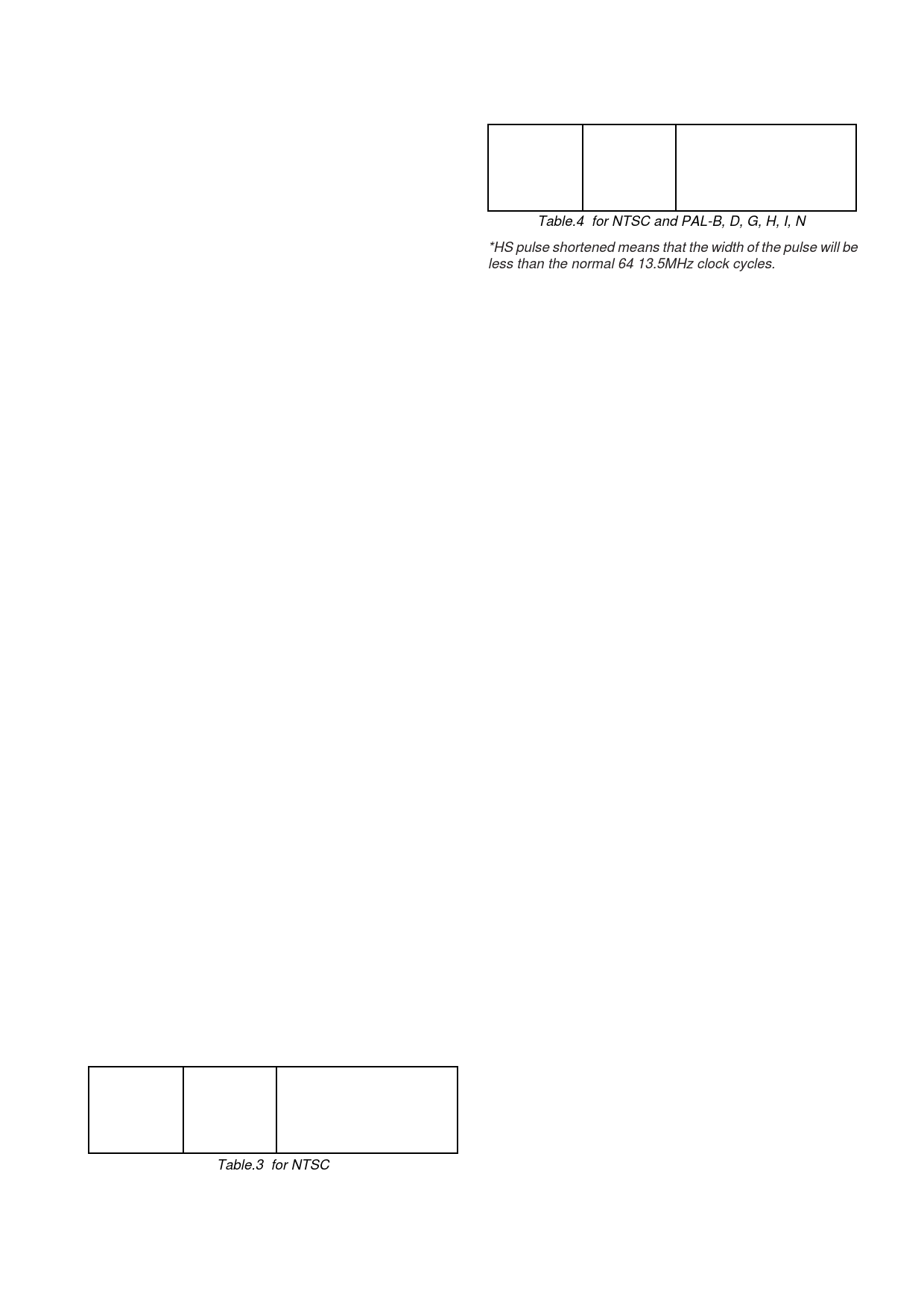
NCK
0 to 120
121 to 138
184 to 857
HSOFF
Comment
126 to 6
HS normal (64 cks)
863 to 801
HS pulse shortened*
800 to 127
HS normal (64 cks)
Table.3 for NTSC
NCK
HSOFF
Comment
0 to 131
137 to 6
HS normal (64 cks)
132 to 194 869 to 807
HS pulse shortened*
195 to 863 806 to 138
HS normal (64 cks)
Table.4 for NTSC and PAL-B, D, G, H, I, N
*HS pulse shortened means that the width of the pulse will be
less than the normal 64 13.5MHz clock cycles.
NCK = number of 13.5MHz clock cycles between the falling
edge of HS and Cb0 (first data I/P on PD7-0) see fig. 4.
Decreasing HSOFF advances the HS pulse (numbers are in
decimal).
The interruption in the sequence of values is because the HS
signal is jumping across a line boundary to the previous line as
the offset is increased. The register default value is 7EH and
this sets Nck to 0, ie. the HS negative edge and Cb0 are co-
incident in NTSC mode.
Video Blanking
The VP531/VP551 automatically performs standard
composite video blanking. Lines 1-9, 264-272 inclusive, as
well as the last half of line 263 are blanked in NTSC mode. In
PAL mode, lines 1-5, 311-318, 624-625 inclusive, as well as
the last half of line 623 are blanked.
The V bit within REC656 defines the video blanking when
TRSEL (bit 0 of GPSCTL register) is set low. When in
MASTER mode with TRSEL set high the video encoder is still
enabled. Therefore if these lines are required to be blank they
must have no video signal input.
Interpolator
The luminance and chrominance data are separately
passed through interpolating filters to produce output
sampling rates double that of the incoming pixel rate. This
reduces the sinx/x distortion that is inherent in the digital to
analog converters and also simplifies the analog
reconstruction filter requirements.
Digital to Analog Converters
The VP531/VP551 contains two 9 bit digital to analog
converters which produce the analog video signals. The
DACs use a current steering architecture in which bit currents
are routed to one of two outputs; thus the DAC has true and
complementary outputs. The use of identical current sources
and current steering their outputs means that monotonicity is
guaranteed. An on-chip voltage reference of 1.05V (typ.)
provides the necessary biasing, if required this can be
overridden by an external reference.
The full-scale output currents of the DACs is set by
external resistors between the DACGAIN and VSS pins. An
on-chip loop amplifier stabilises the full-scale output current
against temperature and power supply variations.
By summing the complementary luma and chroma DAC
current outputs an inverted composite output is generated.
Note that this signal has a DC offset and therefore usually
needs to be capacitively coupled. The analog outputs of the
VP531/VP551 are capable of directly driving doubly
terminated 75Ω co-axial cable. If it is required only to drive a
single 75Ω load then DACGAIN resistor is simply doubled.
9
Share Link: 