VP551E View Datasheet(PDF) - Mitel Networks
Part Name
Description
View to exact match
VP551E Datasheet PDF : 16 Pages
| |||
VP531E/VP551E
Luminance, Chrominance and Composite Video Outputs
The Luminance video output (LUMAOUT pin 54) drives a
37.5Ω load at 1.0V, sync tip to peak white. It contains only the
luminance content of the image plus the composite sync
pulses. In the NTSC mode, a set-up level (pedestal) offset can
be added during the active video portion of the raster. The
pedestal is programmed by PEDEN bit in VOCR register.
The Chrominance video output (CHROMAOUT pin 58)
drives a 37.5Ω load at levels proportional in amplitude to the
luma output (40 IRE pk-pk burst). This output has a fixed offset
current which will produce approximately a 0.5V DC bias
across the 37.5Ω load. Burst is injected with the appropriate
timing relative to the luma signal.
The inverted composite video output (COMPOUTB pin
56) will also drive a 37.5Ω loas at 1.0V, sync tip to peak white.
It contains both the luminance and chrominance content of the
signal plus the composite sync pulses.
Output sinx/x compensation filters are required on all
video output, as shown in the typical application diagram, see
figs. 6 & 7.
Genlock using REFSQ input
The VP531/VP551 can be Genlocked to another video
source by setting GENLKEN high (in GPSCTL register) and
feeding a phase coherent sub carrier frequency signal into
REFSQ. Under normal circumstances, REFSQ will be the
same frequency as the sub carrier. But by setting FSC4SEL
high (in GPSCTL register), a 4 x sub carrier frequency signal
may be input to REFSQ. In this case, the Genlock circuit can
be reset to the required phase of REFSQ, by supplying a pulse
to SCSYNC (pin 9). The frequency of SCSYNC can be at sub
carrier frequency, but once per line, or once per field could be
adequate, depending on the application. When GENLKEN is
SET high, the direction setting of bit 6 of the GPPCTL register
is ignored.
PALID Input
When in Genlock mode with GENLKEN set high (in
GPSCTL register), the VP531 requires a PAL phase
identification signal, to define the correct phase on every line.
This is supplied to PALID input (pin 10), High = -135° and low
= +135°. The signal is asynchronous and should be changed
before the sub carrier burst signal. PALID input is enabled by
setting PALIDEN high (in GPSCTL register). When
GENLKEN is high, the direction setting of bit 7 of the GPPCTL
register is ignored
Master Reset
The VP531/VP551 must be initialised with the RESET pin
34. This is an asynchronous active low signal and must be
active for a minimum of 200ns in order for the VP531 to be
reset. The device resets to line 64, start of horizontal sync (i.e.
line blanking active). There is no on-chip power on reset
circuitry.
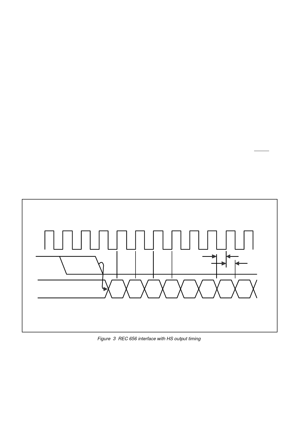
PXCK Input (27MHz)
HS
Nck=2
Nck=0
t SU; PD
t HD; PD
Cb0 Y0 Cr0 Y1 Cb1 Y2 Cr1 Y3
Pixel Data Input (PD[7,0])
Figure 3 REC 656 interface with HS output timing
10
Share Link: 