RTL8130 View Datasheet(PDF) - Realtek Semiconductor
Part Name
Description
View to exact match
RTL8130 Datasheet PDF : 55 Pages
| |||
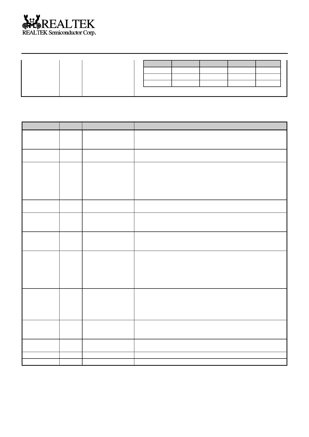
RTL8130 Preliminary
LEDS1-0
LED0
LED1
LED2
00
TX/RX
LINK100
LINK10
01
TX/RX
LINK10/100
FULL
10
TX
LINK10/100
RX
During power down mode, the LED’s are OFF.
11
TX
LINK100
LINK10
4.6 100/10 Mbps MII Interface(MII mode, 18 pins)
Symbol
TXC
Type
I
TXEN
O
TXD3
O
TXD2
TXD1
TXD0(BNC)
RXC
I
COL
I
RXDV
I
RXD3
I
RXD2
RXD1
RXD0(AUI)
RXER
I
MDC
O
MDIO
I/O
MLink
I
MFDup
I
Pin No
86
85
79
80
81
83
88
78
89
93
92
91
90
87
96
95
77
76
Description
Transmit Clock: TXC is a continuous clock that provides a timing
reference for the transfer of TXD[3:0], TEN. In MII mode, it uses the
25 MHz or 2.5 MHz supplied by the external PMD device.
Transmit Enable: Indicates the presence of valid nibble data on
TXD[3:0].
MII mode: (bit1=0, Config3)
Transmit Data(MII mode, Config3 bit1=1): Four parallel transmit
data lines which are driven synchronous to the TXC for
transmission by the external physical layer chip.
AUI mode: (bit1=1, Config3)
TXD0=BNC
Receive Clock: This is a continuous clock that is recovered from the
incoming data. RXC is 25MHz in 100Mbps and 2.5Mhz in 10Mbs.
Collision Detected: This signal is asserted high synchronously by the
external physical unit upon detection of a collision on the medium. It
will remain asserted as long as the collision condition persists.
Receive Data Valid: Data valid is asserted by an external PHY when
receive data is present on the RXD[3:0] lines, and it is deasserted at
the end of the packet. This signal is valid on the rising of the RXC.
MII mode: (bit1=1, Config3)
Receive Data: This is a group of 4 data signals aligned on nibble
boundaries which are driven synchronous to the RXC by the
external physical unit.
AUI mode: (bit1=0, Config3)
RXD0= AUI.
Receive Error: This pin is asserted to indicate that invalid symbol has
been detected in 100Mbps MII mode. This signal is synchronized to
RXC and can be asserted for a minimum of one receive clock. When
asserted during a packet reception, it sets the ISE bit of the RSR
register in the header of the Rx packet.
Management Data Clock: Synchronous clock to the MDIO
management data input/output serial interface which may be
asynchronous to transmit and receive clocks.
Management Data: Bi-directional signal used to transfer management
information.
MII link status notification
MII full-duplex status notification
1999/5/30
7
Ver.1.1
Share Link: 