UPD45128163-I-E View Datasheet(PDF) - Elpida Memory, Inc
Part Name
Description
View to exact match
UPD45128163-I-E
Elpida Memory, Inc

UPD45128163-I-E Datasheet PDF : 86 Pages
| |||
µPD45128163-I-E
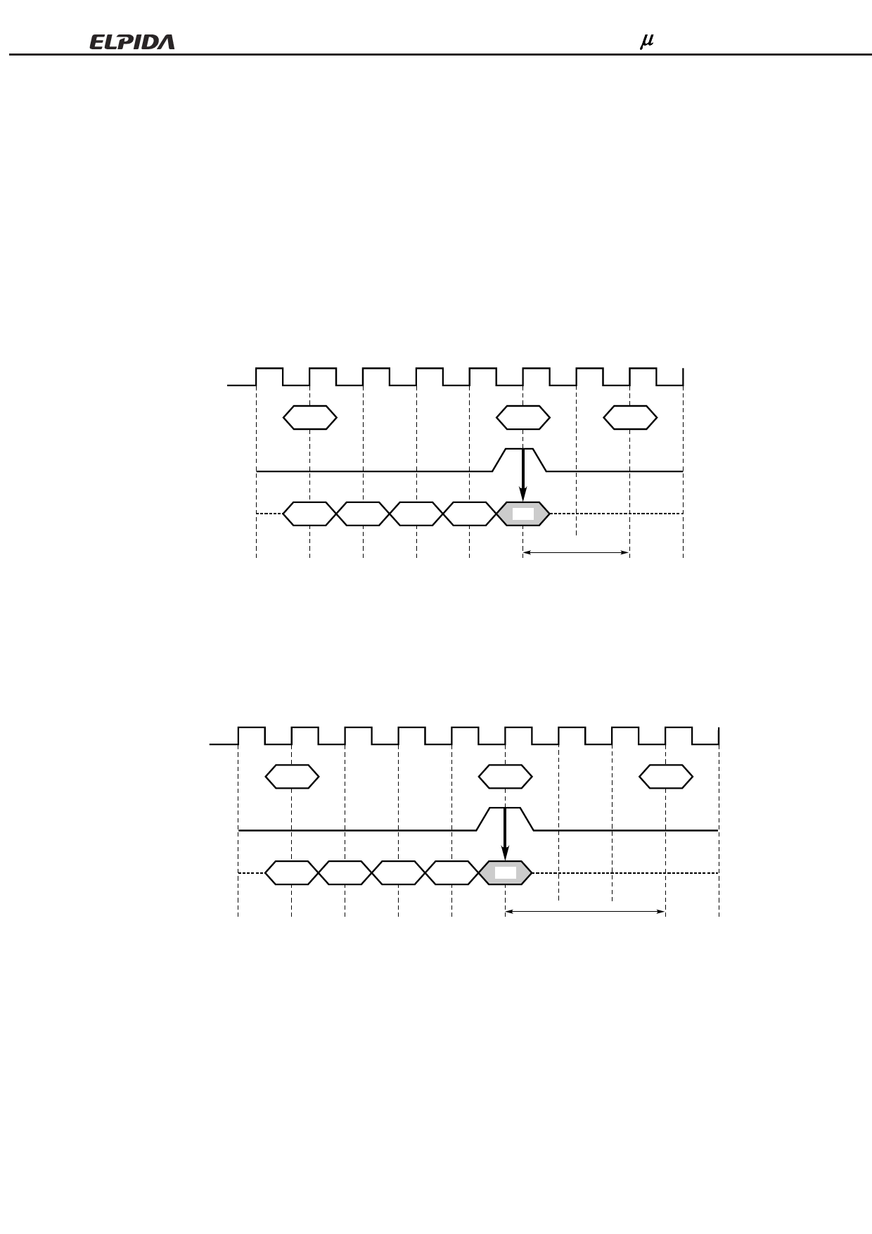
12.2.2 Precharge Termination in WRITE Cycle
During a write cycle, the burst write operation is terminated by a precharge command.
When the precharge command is issued, the burst write operation is terminated and precharge starts.
The same bank can be activated again after tRP from the precharge command.
To issue a precharge command, tRAS must be satisfied.
When /CAS latency is 2, the write data written prior to the precharge command will be correctly stored. However,
invalid data may be written at the same clock as the precharge command. To prevent this from happening, DQM must
be high at the same clock as the precharge command. This will mask the invalid data.
Burst length = X, /CAS latency = 2
T0
T1
T2
T3
T4
T5
T6
T7
CLK
Command
WRITE
PRE
ACT
DQM
DQ
Hi-Z
D1
D2
D3
D4
D5
tRP
(tRAS must be satisfied)
When /CAS latency is 3, the write data written prior to the precharge command will be correctly stored. However,
invalid data may be written at the same clock as the precharge command. To prevent this from happening, DQM must
be high at the same clock as the precharge command. This will mask the invalid data.
Burst length = X, /CAS latency = 3
T0
T1
T2
T3
T4
T5
T6
T7
T8
CLK
Command
WRITE
PRE
ACT
DQM
DQ
D1
D2
D3
D4
D5
Hi-Z
tRP
(tRAS must be satisfied)
Data Sheet E0729N10 (Ver. 1.0)
31
Share Link: