MM912G634CM1AE View Datasheet(PDF) - Freescale Semiconductor
Part Name
Description
View to exact match
MM912G634CM1AE Datasheet PDF : 345 Pages
| |||
Freescale Semiconductor
Advance Information
Document Number: MM912_634D1
Rev. 4.0, 5/2011
Integrated S12 Based Relay
Driver with LIN
The MM912G634 (48 kB) and MM912H634 (64 kB) are
integrated single package solutions that integrates an HCS12
microcontroller with a SMARTMOS analog control IC. The Die
to Die Interface (D2D) controlled analog die combines system
base chip and application specific functions, including a LIN
transceiver.
Features
• 16-Bit S12 CPU, 64/48 kByte P-FLASH,
• 6.0 kByte RAM; 4/2 kByte D-FLASH
• Background debug (BDM) & debug module (DBG)
• Die to Die bus interface for transparent memory mapping
• On-chip oscillator & two independent watchdogs
• LIN 2.1 Physical Layer Interface with integrated SCI
• 10 digital MCU GPIOs shared with SPI (PA7…0, PE1…0)
• 10-Bit, 15 Channel - Analog to Digital Converter (ADC)
• 16-Bit, 4 Channel - Timer Module (TIM16B4C)
• 8-Bit, 2 Channel - Pulse width modulation module (PWM)
MM912_634
48-PIN LQFP, 7.0 mm x 7.0 mm
AE SUFFIX: Exposed Pad Option
AP SUFFIX: Non Exposed Pad Option
ORDERING INFORMATION
See Page 2.
• Six high voltage / Wake-up inputs (L5…0)
• Three low voltage GPIOs (PB2…0)
• Low power modes with cyclic sense & forced wake-up
• Current sense module with selectable gain
• Reverse battery protected voltage sense module
• Two protected low side outputs to drive inductive loads
• Two protected high side outputs
• Chip temperature sensor
• Hall sensor supply & integrated voltage regulator(s)
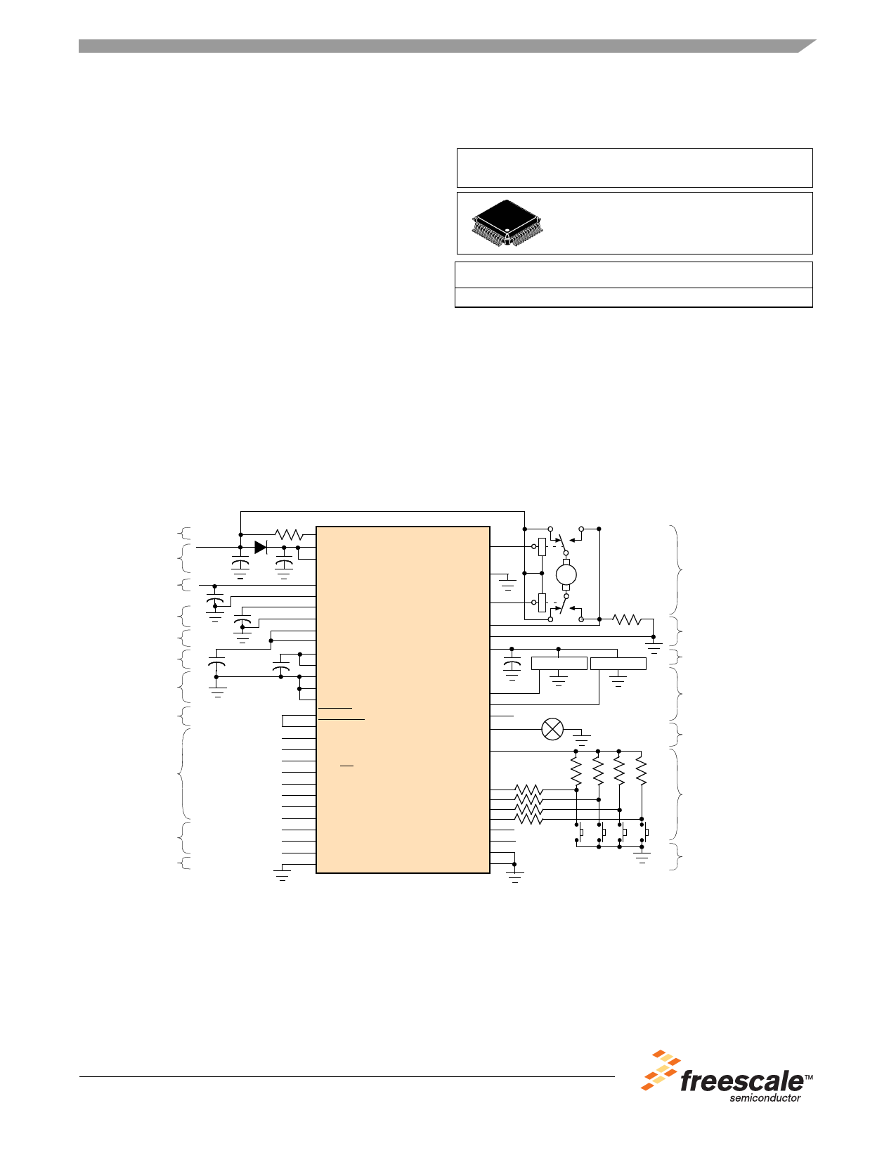
Battery Sense
Power Supply
LIN Interface
ADC Supply
2.5 V Suppy
5.0 V Supply
Digital Ground
Reset
5.0 V Digital I/O
Debug and External
Oscillator
MCU Test
VSENSE
VS1
VS2
MM912_634 LS1
PGND
LIN
LGND
ADC25
LS2
AGND
VDD
VDDD2D
VDDX
ISENSEH*
ISENSEL*
HSUP
VDDRX
DGND
VSSD2D
VSSRX
PTB0/AD0/RX/TIM0CH0
PTB1/AD1/TX/TIM0CH1
RESET PTB2/AD2/PWM/TIM0CH2
RESET_A
HS1
PA0/MISO
PA1/MOSI
PA2/SCK
HS2*
PA3/SS
PA4
PA5
PA6
L0
L1
L2
PA7
L3
BKGD/MODC
L4*
PE0/EXTAL
L5*
PE1/XTAL
TCLK
TEST
TEST_A
* Feature not availablre in all Analog Options
M
Hall Sensor Hall Sensor
Figure 1. Simplified Application Diagram
Low Side Drivers
Current Sense Moe
Hall Sensor Supply
5.0 V GPI/O with optional
pull-up (shared with ADC,
PWM, Timer, and SCI)
12 V Light/LED and
Switch Supply
Analog/Digita inputs
(High Voltage and Wake-up
capable)
Analog Test
This document contains certain information on a new product. Specifications and information herein
are subject to change without notice.
© Freescale Semiconductor, Inc., 2010-2011. All rights reserved.
Share Link: 