MM912G634CM1AE View Datasheet(PDF) - Freescale Semiconductor
Part Name
Description
View to exact match
MM912G634CM1AE Datasheet PDF : 345 Pages
| |||
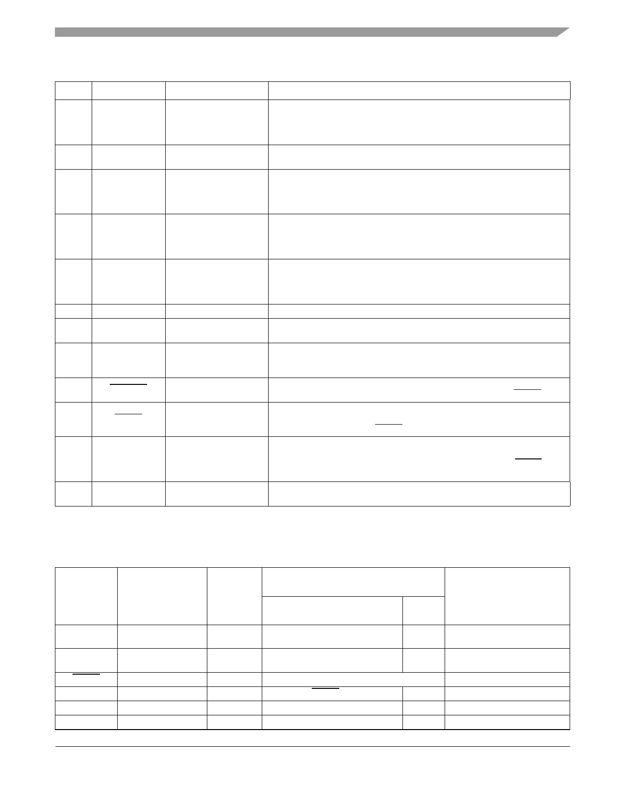
Pin Assignment
Pin #
37
38
39
40
41
42
43
44
45
46
47
48
Pin Name
LS1
PGND
LS2
ISENSEL
ISENSEH
NC
TEST_A
TCLK
RESET_A
RESET
BKGD
PA7
Table 4. MM912_634 Pin Description
Formal Name
Description
Low Side Output 1
Low Side output 1 used to drive small inductive loads like relays. The output is
short-circuit protected, includes active clamp circuitry and can be also controlled by
the PWM module.
See Section 4.13, “Low Side Drivers - LSx
Power Ground Pin
This pin is the device Low Side Ground connection. DGND, LGND and AGND are
internally connected to PGND via a back to back diode.
Low Side Output 2
Low Side output 2 used to drive small inductive loads like relays. The output is
short-circuit protected, includes active clamp circuitry and can be also controlled by
the PWM module.
See Section 4.13, “Low Side Drivers - LSx
Current Sense Pin L
Current Sense differential input “Low”. This pin is used in combination with
ISENSEH to measure the voltage drop across a shunt resistor. See Section 4.21,
“Current Sense Module - ISENSE. Note: This pin function is not available on all
device configurations.
Current Sense Pin H
Current Sense differential input “High”. This pin is used in combination with
ISENSEL to measure the voltage drop across a shunt resistor. Section 4.21,
“Current Sense Module - ISENSE. Note: This pin function is not available on all
device configurations.
Not connected
This pin is reserved for alternative function and should be left floating.
Test Mode
Analog die Test Mode pin for Test Mode only. This pin must be grounded in user
mode!
Test Clock Input
Test Mode Clock Input pin for Test Mode only. The pin can be used to disable the
internal watchdog for development purpose in user mode. See Section 4.10,
“Window Watchdog. The pin is recommended to be grounded in user mode.
Reset I/O
Bidirectional Reset I/O pin of the analog die. Active low signal. Internal pull-up. VDDX
based. See Section 4.8, “Resets. To be externally connected to the RESET pin.
MCU Reset
The RESET pin is an active low bidirectional control signal. It acts as an input to
initialize the MCU to a known start-up state, and an output when an internal MCU
function causes a reset. The RESET pin has an internal pull-up device to EVDDX.
MCU Background Debug
and Mode
The BKGD/MODC pin is used as a pseudo-open-drain pin for the background
debug communication. It is used as MCU operating mode select pin during reset.
The state of this pin is latched to the MODC bit at the rising edge of RESET. The
BKGD pin has a pull-up device.
MCU PA7
General purpose port A input or output pin 7. See Section 4.28, “Port Integration
Module (S12IPIMV1)
2.2 MCU Die Signal Properties
This section describes the external MCU signals. It includes a table of signal properties.
Table 5. Signal Properties Summary
Pin
Name
Function 1
PE0
PE1
RESET
TEST
BKGD
PA7
Pin
Name
Function 2
EXTAL
XTAL
—
—
MODC
—
Freescale Semiconductor
Power
Supply
Internal Pull
Resistor
CTRL
VDDRX
VDDRX
VDDRX
N.A.
VDDRX
VDDRX
PUPEE/
OSCPINS_EN
PUPBE/
OSCPINS_EN
PULLUP
RESET pin
BKPUE
NA
MM912_634 Advance Information, Rev. 4.0
Reset
State
DOWN
DOWN
DOWN
UP
NA
Description
Port E I/O, Oscillator pin
Port E I/O, Oscillator pin
External reset
Test input
Background debug
Port A I/O
11
Share Link: 