FS50UM-3-A8 View Datasheet(PDF) - Renesas Electronics
Part Name
Description
View to exact match
FS50UM-3-A8 Datasheet PDF : 7 Pages
| |||
FS50UM-3
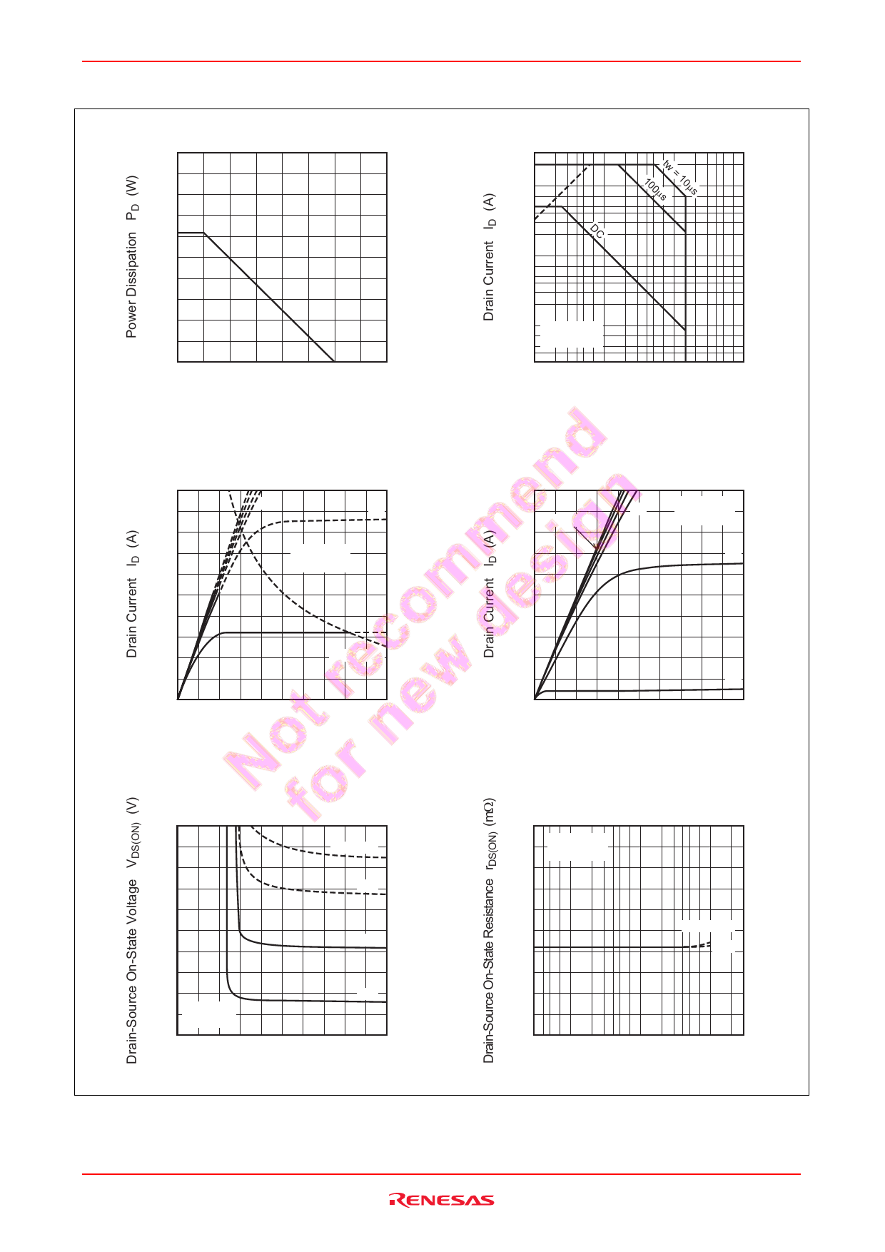
Performance Curves
Power Dissipation Derating Curve
200
160
120
80
40
0
0
50
100
150
200
Case Temperature Tc (°C)
Output Characteristics (Typical)
VGS = 20V 10V 8V
100
7V
6V
80
Tc = 25°C
Pulse Test
60
40
5V
20
PD = 125W
0
0
1.0 2.0 3.0 4.0 5.0
Drain-Source Voltage VDS (V)
On-State Voltage vs.
Gate-Source Voltage (Typical)
2.0
ID = 100A
1.6
80A
1.2
50A
0.8
0.4
Tc = 25°C
Pulse Test
0
0
4
8
20A
12 16 20
Gate-Source Voltage VGS (V)
Rev.2.00 Aug 07, 2006 page 3 of 6
Maximum Safe Operating Area
3
2
102
7
tw
100µs = 10µs
5
3
2
DC
101
7
5
3
2
100 Tc = 25°C
7
5
Single Pulse
3100 2 3 5 7 101 2 3
5 7 102 2 3
5 7 103
Drain-Source Voltage VDS (V)
Output Characteristics (Typical)
50
VGS = 20V
40
10V 7V
6V
Tc = 25°C
Pulse Test
5V
30
20
10
4V
0
0 0.4 0.8 1.2 1.6 2.0
Drain-Source Voltage VDS (V)
On-State Resistance vs.
Drain Current (Typical)
40
Tc = 25°C
Pulse Test
32
24
VGS = 10V
16
20V
8
0
3 5 7 100 2 3 5 7 101 2 3 5 7 102 2 3
Drain Current ID (A)
Share Link: 