EDS2516APTA-75TI-E View Datasheet(PDF) - Elpida Memory, Inc
Part Name
Description
View to exact match
EDS2516APTA-75TI-E Datasheet PDF : 52 Pages
| |||
DATA SHEET
256M bits SDRAM
WTR (Wide Temperature Range)
EDS2516APTA-TI-E (16M words × 16 bits)
Description
The EDS2516APTA is a 256M bits SDRAM organized
as 4194304 words × 16 bits × 4 banks. All inputs and
outputs are referred to the rising edge of the clock
input. It is packaged in 54-pin plastic TSOP (II).
Features
• 3.3V power supply
• Clock frequency: 133MHz (max.)
• LVTTL interface
• Single pulsed /RAS
• ×16 organization
• 4 banks can operate simultaneously and
independently
• Burst read/write operation and burst read/single write
operation capability
• Programmable burst length (BL): 1, 2, 4, 8, full page
• 2 variations of burst sequence
Sequential (BL = 1, 2, 4, 8)
Interleave (BL = 1, 2, 4, 8)
• Programmable /CAS latency (CL): 2, 3
• Byte control by UDQM and LDQM
• Refresh cycles: 8192 refresh cycles/64ms
• 2 variations of refresh
Auto refresh
Self refresh
• TSOP (II) package with lead free solder (Sn-Bi)
• Wide temperature range
Ambient temperature range: –40 to +85°C
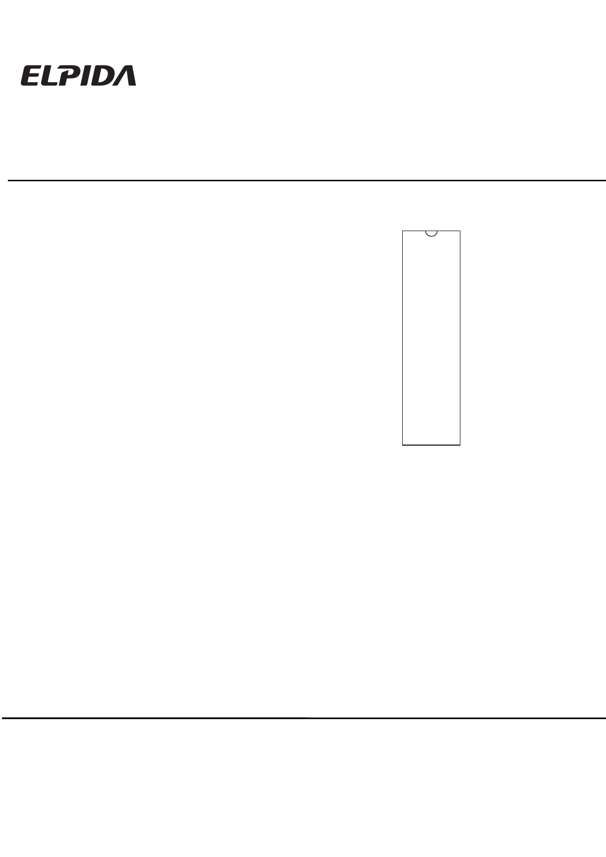
Pin Configurations
/xxx indicates active low signal.
54-pin plastic TSOP (II)
VDD
DQ0
VDDQ
DQ1
DQ2
VSSQ
DQ3
DQ4
VDDQ
DQ5
DQ6
VSSQ
DQ7
VDD
LDQM
/WE
/CAS
/RAS
/CS
BA0
BA1
A10
A0
A1
A2
A3
VDD
1
54
2
53
3
52
4
51
5
50
6
49
7
48
8
47
9
46
10
45
11
44
12
43
13
42
14
41
15
40
16
39
17
38
18
37
19
36
20
35
21
34
22
33
23
32
24
31
25
30
26
29
27
28
(Top view)
VSS
DQ15
VSSQ
DQ14
DQ13
VDDQ
DQ12
DQ11
VSSQ
DQ10
DQ9
VDDQ
DQ8
VSS
NC
UDQM
CLK
CKE
A12
A11
A9
A8
A7
A6
A5
A4
VSS
A0 to A12, Address input
BA0, BA1 Bank select address
DQ0 to DQ15 Data-input/output
/CS
Chip select
/RAS
Row address strobe
/CAS
Column address strobe
/WE
Write enable
UDQM,LDQM Input/output mask
CKE
Clock enable
CLK
Clock input
VDD
Power for internal circuit
VSS
Ground for internal circuit
VDDQ
Power for DQ circuit
VSSQ
Ground for DQ circuit
NC
No connection
Document No. E0677E10 (Ver. 1.0)
Date Published March 2005 (K) Japan
Printed in Japan
URL: http://www.elpida.com
Elpida Memory, Inc. 2005
Share Link: 