MAX8830EWET(2007) View Datasheet(PDF) - Maxim Integrated
Part Name
Description
View to exact match
MAX8830EWET Datasheet PDF : 15 Pages
| |||
UCSP
BUMP
A1
A2
A3
A4
C1
B1
B2
D1
B3
B4
C2
C3
C4
D2
D3
D4
LED Light Management IC in
2.5mm x 2.5mm UCSP
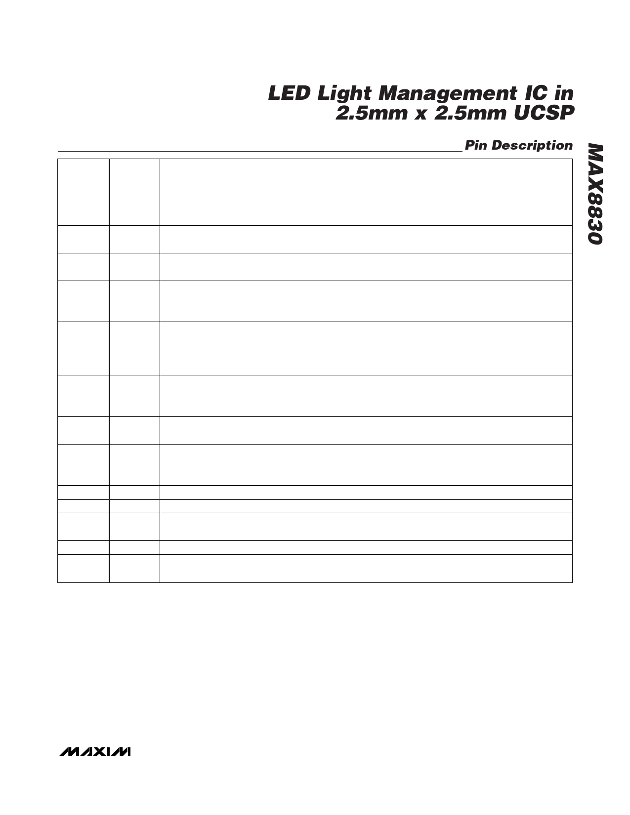
Pin Description
NAME
FUNCTION
FLED
PGND
LX
OUT
LED1
LED2
LED3
LED4
MVON
IN
FLEN
SCL
COMP
GND
SDA
VDD
Flash LED Current-Sink Regulator. Current flowing into FLED is based on the internal I2C registers.
Connect FLED to the cathode of an external flash LED or LED module. FLED is high impedance during
shutdown. If unused, FLED may be shorted to ground or left unconnected.
Power Ground. Connect PGND to GND and to the input capacitor ground. Connect PGND to the PCB
ground plane.
Inductor Connection. Connect LX to the switched side of the inductor. LX is internally connected to the
drains of the internal MOSFETs. LX is high impedance in shutdown.
Regulator Output. Connect OUT to the anodes of the external LEDs. OUT can also be used to supply
other circuits, such as audio amplifiers. Bypass OUT to PGND with a 10µF or larger ceramic capacitor.
During shutdown, VOUT is one diode drop below the VIN.
LED Current-Sink Regulators. Current flowing into LED_ is based on the internal I2C registers. Connect
LED_ to the cathodes of external LEDs. LED_ is high impedance during shutdown. If unused, LED_ can
be shorted to ground or left unconnected.
Movie On Logic Input. Connect to VDD or drive with logic 1 to enable the movie mode. The FLED movie
current is set in the I2C registers. Connect to GND or drive with logic 0 to turn off the movie mode. The
movie mode is also enabled through the I2C interface.
Analog Supply Voltage Input. The input voltage range is 2.7V to 5.5V. Bypass IN to GND and PGND with
a 10µF ceramic capacitor as close as possible to the IC. IN is high impedance during shutdown.
Flash Enable Logic Input. A transition from logic 0 to logic 1 on FLEN initiates the flash mode. The flash
duration and FLED flash current are set in I2C registers. The flash mode terminates when either FLEN
transitions back to logic 0 or after the flash-duration timer expires.
I2C Clock Input. Data is read on the rising edge of SCL.
Compensation Input. See the COMP Network Selection section for details.
Analog Ground. Connect GND to PGND and to the input capacitor ground. Connect GND to the PCB
ground plane.
I2C Data Input. Data is read on the rising edge of SCL.
Logic Input Supply Voltage. Connect VDD to the logic supply driving SCL, SDA, MVON, and FLEN.
Bypass VDD to GND with a 0.1µF ceramic capacitor. Setting VDD = 0 places the part in shutdown.
_______________________________________________________________________________________ 7
Share Link: 