MAX8830EWET(2007) View Datasheet(PDF) - Maxim Integrated
Part Name
Description
View to exact match
MAX8830EWET Datasheet PDF : 15 Pages
| |||
LED Light Management IC in
2.5mm x 2.5mm UCSP
I2C Serial Interface
The step-up converter OUT voltage, FLED flash current
and duration, FLED movie current, and LED_ individual
currents are set using the I2C serial interface. Each cur-
rent level is individually programmable (including off)
with a single command (see Tables 1, 2, and 3). While
the flash current is set through I2C, current does not
flow until the FLEN input is logic 1, as described in the
Flash Current-Sink Regulator (FLED, MVON, FLEN)
section. By default, the movie current is turned on when
a nonzero setting is programmed through I2C.
Alternately, by setting a bit in the “other” register, the
movie mode current may also be gated by logic 1 at
the MVON input.
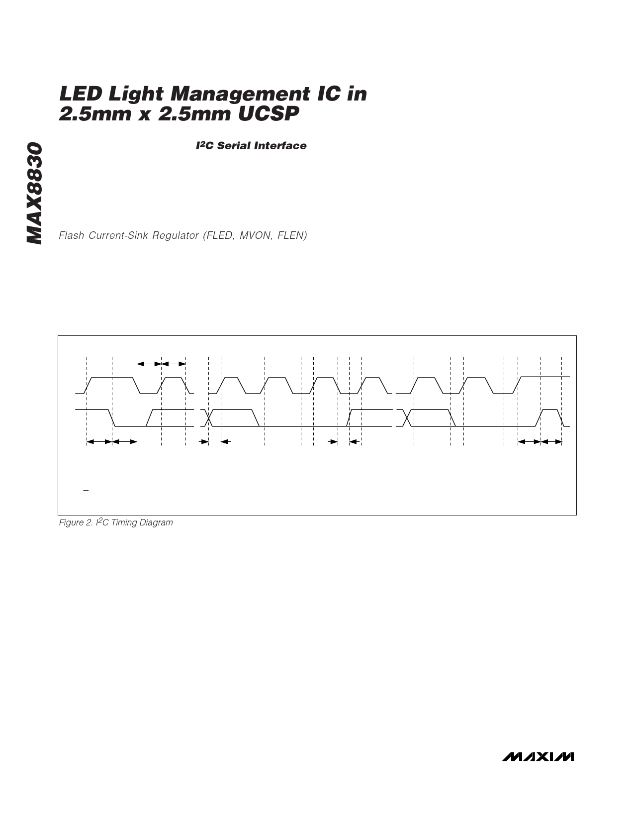
The I2C serial interface consists of a serial-data line
(SDA) and a serial-clock line (SCL). Standard I2C write-
byte commands are used. Figure 2 shows a timing dia-
gram for the I2C protocol. The MAX8830 is a slave-only
device, relying upon a master to generate a clock sig-
nal. The master (typically a microprocessor) initiates
data transfer on the bus and generates SCL to permit
data transfer. A master device communicates to the
MAX8830 by transmitting the proper 8-bit address
(0x94) followed by the 8-bit control byte. Each 8-bit
control byte consists of a command code (usually
3-bits) with the remaining bits (usually 5 bits) as data
(see Table 1). Each transmit sequence is framed by a
START (A) condition and a STOP (L) condition. Each
word transmitted over the bus is 8 bits long and is
always followed by an acknowledge clock pulse.
A
tLOW B tHIGH
C
D
EF
G
SCL
SDA
tSU_STA tHD_STA
A = START CONDITION
B = MSB OF ADDRESS CLOCKED INTO SLAVE
C = LSB OF ADDRESS CLOCKED INTO SLAVE
D = R/W BIT CLOCKED INTO SLAVE
E = SLAVE PULLS SMBDATA LINE LOW
Figure 2. I2C Timing Diagram
tSU_DAT
tHD_DAT
F = ACKNOWLEDGE BIT CLOCKED INTO MASTER
G = MSB OF DATA CLOCKED INTO SLAVE (OP/SUS BIT)
H = LSB OF DATA CLOCKED INTO SLAVE
I = SLAVE PULLS SMBDATA LINE LOW
H
IJ
K
LM
tSU_STO tBUF
J = ACKNOWLEDGE CLOCKED INTO MASTER
K = ACKNOWLEDGE CLOCK PULSE
L = STOP CONDITION, DATA EXECUTED BY SLAVE
M = NEW START CONDITION
10 ______________________________________________________________________________________
Share Link: 