CDP1877 View Datasheet(PDF) - Intersil
Part Name
Description
View to exact match
CDP1877 Datasheet PDF : 10 Pages
| |||
CDP1877, CDP1877C
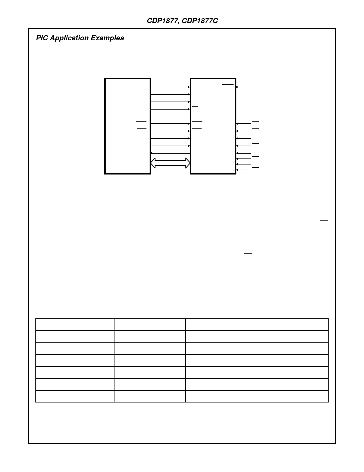
PIC Application Examples
Example 1 - Single PIC Application
Figure 2 shows all the connections required between CPU
and PIC to handle eight levels of interrupt control.
MA7
MA6
MA5
CPU MA4
CDP1802
MWR
MRD
TPA
TPB
INT
BUS
CS/AX
CASC
VDD
CS/AY
CS
CS
PIC
CDP1877
MWR
IR7
MRD
IR6
TPA
IR5
TPB
IR4
INT
IR3
IR2
BUS
IR1
IR0
FIGURE 2. PIC AND CPU CONNECTION DIAGRAM
Programming
Programming the PIC consists of the following steps:
1. Disable interrupt at CPU
2. Reset Master Interrupt Bit, B3, of Control Register.
3. Write a “1” into the Interrupt Input bit location of the Mask
Register, if masking is desired.
4. Write the High-Order Address byte into the Page
Register.
5. Write the Low-Order Address and the vector interval into
the Control Register.
6. Program R(1) of the CPU to point to the PIC so that the
Long Branch instruction can be read from the PIC during
the Interrupt Service routine.
Values for Example 1 with LOCATION 84E0 arbitrarily cho-
sen as the Vector Address with interval of eight bytes, IR4
pending, is shown in Table 1.
In deriving the above addresses, all Don’t Care bits are
assumed to be 0.
When an INTERRUPT (IR4) is received by the CPU, it will
address the PIC and will branch to the interrupt service
routine.
The three bytes generated by the PIC will be:
1st Byte = C0H
2nd Byte = 84H
3rd Byte = E0H
TABLE 1. REGISTER ADDRESS VALUES
REGISTER
REGISTER ADDRESS
OPERATION
DATA BYTE
MASK
CONTROL
PAGE
STATUS
POLLING
R(1) (IN CPU)
E000H
E040H
E080H
E000H
E040H
E080H
WRITE
WRITE
WRITE
READ
READ
-
00H
CEH
84H
10H
E0H
-
4-88
Share Link: 