D4564163G5 View Datasheet(PDF) - Elpida Memory, Inc
Part Name
Description
View to exact match
D4564163G5 Datasheet PDF : 85 Pages
| |||
µPD4564441, 4564841, 4564163
2. Commands
Mode register set command
(/CS, /RAS, /CAS, /WE = Low)
The µPD4564xxx has a mode register that defines how the device
operates. In this command, A0 through A13 are the data input pins.
After power on, the mode register set command must be executed to
initialize the device.
The mode register can be set only when all banks are in idle state.
During 2 CLK (tRSC) following this command, the µPD4564xxx cannot
accept any other commands.
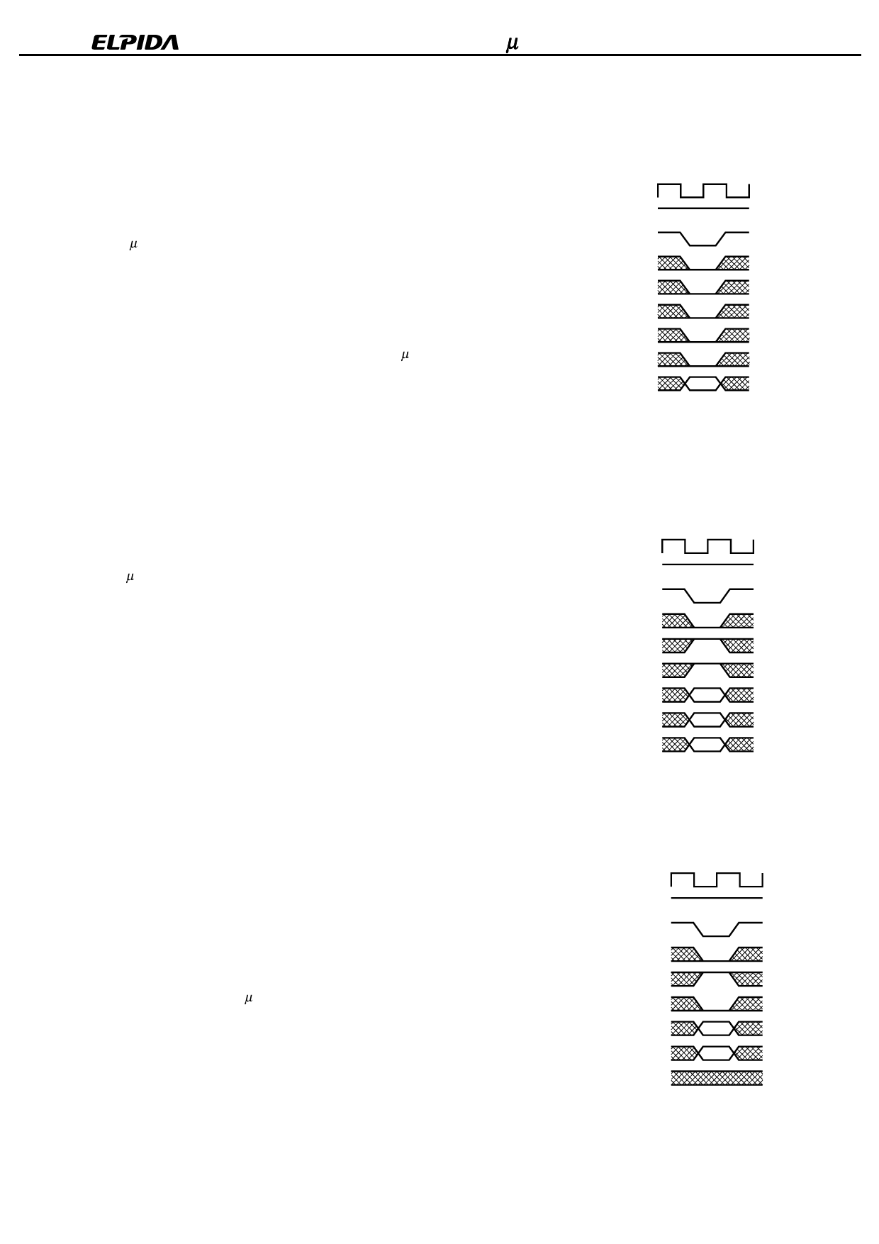
Fig.1 Mode register set command
CLK
CKE H
/CS
/RAS
/CAS
/WE
A12, A13
A10
Add
Activate command
(/CS, /RAS = Low, /CAS, /WE = High)
The µPD4564xxx has four banks, each with 4,096 rows.
This command activates the bank selected by A12 and A13 (BS) and a
row address selected by A0 through A11.
This command corresponds to a conventional DRAM’s /RAS falling.
Fig.2 Row address strobe and
bank activate command
CLK
CKE
/CS
/RAS
/CAS
/WE
A12, A13
(Bank select)
A10
Add
H
Row
Row
Precharge command
(/CS, /RAS, /WE = Low, /CAS = High)
This command begins precharge operation of the bank selected by
A12 and A13 (BS). When A10 is High, all banks are precharged,
regardless of A12 and A13. When A10 is Low, only the bank selected
by A12 and A13 is precharged.
After this command, the µPD4564xxx can’t accept the activate
command to the precharging bank during tRP (precharge to activate
command period).
This command corresponds to a conventional DRAM’s /RAS rising.
Data Sheet E0149N10
Fig.3 Precharge command
CLK
CKE H
/CS
/RAS
/CAS
/WE
A12, A13
(Bank select)
A10
(Precharge select)
Add
11
Share Link: 