D4564163G5 View Datasheet(PDF) - Elpida Memory, Inc
Part Name
Description
View to exact match
D4564163G5 Datasheet PDF : 85 Pages
| |||
µPD4564441, 4564841, 4564163
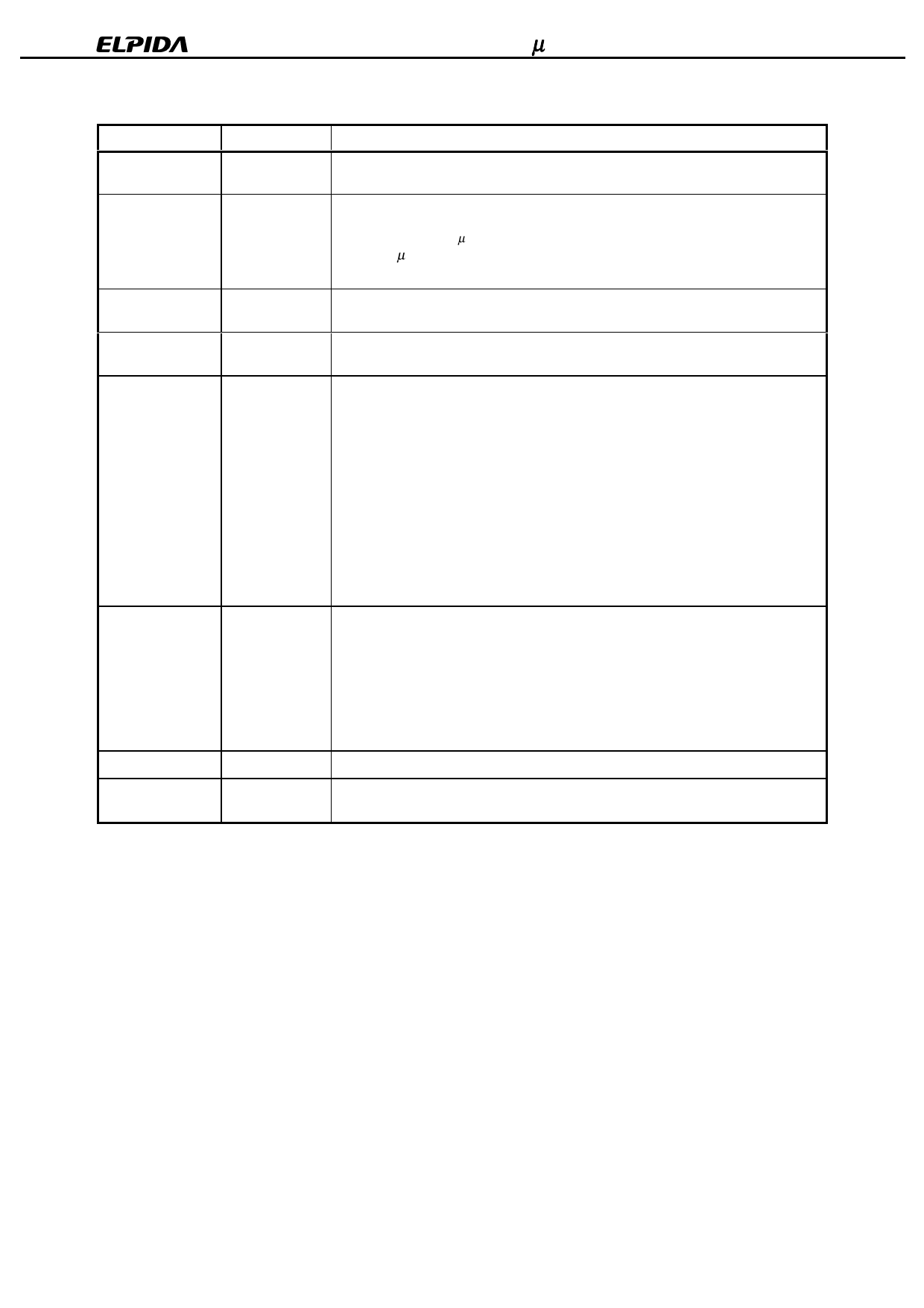
1. Input / Output Pin Function
Pin name
CLK
CKE
/CS
/RAS, /CAS, /WE
A0 - A13
DQM, UDQM,
LDQM
DQ0 - DQ15
Input / Output
Input
Input
Input
Input
Input
Input
Input / Output
Function
CLK is the master clock input. Other inputs signals are referenced to the CLK rising
edge.
CKE determine validity of the next CLK (clock). If CKE is high, the next CLK rising
edge is valid; otherwise it is invalid. If the CLK rising edge is invalid, the internal clock
is not issued and the µPD4564xxx suspends operation.
When the µPD4564xxx is not in burst mode and CKE is negated, the device enters
power down mode. During power down mode, CKE must remain low.
/CS low starts the command input cycle. When /CS is high, commands are ignored
but operations continue.
/RAS, /CAS and /WE have the same symbols on conventional DRAM but different
functions. For details, refer to the command table.
Row Address is determined by A0 - A13 at the CLK (clock) rising edge in the active
command cycle. It does not depend on the bit organization.
Column Address is determined by A0 - A9 at the CLK rising edge in the read or write
command cycle. It depends on the bit organization: A0 - A9 for ×4 device, A0 - A8 for
×8 device, A0 - A7 for ×16 device.
A12 and A13 are the bank select signal (BS). In command cycle, A12 and A13 low
select bank A, A12 low and A13 high select bank B, A12 high and A13 low select bank
C and then A12 and A13 high select bank D.
A10 defines the precharge mode. When A10 is high in the precharge command cycle,
all banks are precharged; when A10 is low, only the bank selected by A12 and A13 is
precharged.
When A10 is high in read or write command cycle, the precharge starts automatically
after the burst access.
DQM controls I/O buffers. In ×16 products, UDQM and LDQM control upper byte and
lower byte I/O buffers, respectively.
In read mode, DQM controls the output buffers like a conventional /OE pin.
DQM high and DQM low turn the output buffers off and on, respectively.
The DQM latency for the read is two clocks.
In write mode, DQM controls the word mask. Input data is written to the memory cell if
DQM is low but not if DQM is high.
The DQM latency for the write is zero.
DQ pins have the same function as I/O pins on a conventional DRAM.
VCC, VSS, VCCQ,
VSSQ
(Power supply)
VCC and VSS are power supply pins for internal circuits. VCCQ and VSSQ are power
supply pins for the output buffers.
10
Data Sheet E0149N10
Share Link: 