AT27LV520-70SU View Datasheet(PDF) - Atmel Corporation
Part Name
Description
View to exact match
AT27LV520-70SU Datasheet PDF : 13 Pages
| |||
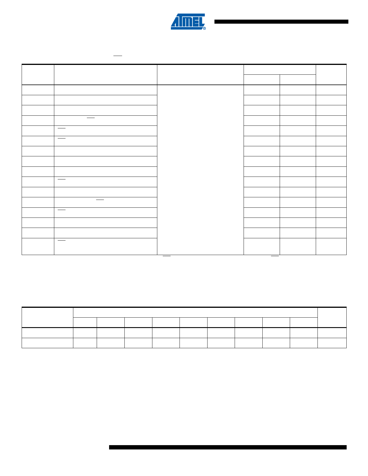
16. AC Programming Characteristics
TA = 25 ± 5° C, VCC = 6.5 ± 0.25V, OE/VPP = 13.0 ± 0.25V
Symbol
Parameter(1)
Test Conditions
Limits
Min
Max
Units
tALE
tLAS
tLAH
tLP
tOES
tOEH
tDS
tDH
tPW
tVR
tVCS
tOE
tDFP
tAS
tAH
tPRT
Notes:
Address Latch Enable Width
500
ns
Latched Address Setup Time
100
ns
Latched Address Hold Time
100
ns
ALE Low to OE/VPP High Voltage Delay
2
µs
OE/VPP Setup Time
Input Rise and Fall Times:
2
µs
OE/VPP Hold Time
(10% to 90%) 20 ns
2
µs
Data Setup Time
Input Pulse Levels:
2
µs
Data Hold Time
0.45V to 2.4V
2
µs
ALE Program Pulse Width(2)
OE/VPP Recovery Time
47.5
52.5
µs
Input Timing Reference Level:
0.8V to 2.0V
2
µs
VCC Setup Time
2
µs
Data Valid from OE/VPP
Output Timing Reference Level:
OE/VPP High to Output Float Delay(3)
0.8V to 2.0V
0
150
ns
130
ns
Address Setup Time
2
µs
Address Hold Time
0
µs
OE/VPP Pulse Rise Time During
Programming
50
ns
1. VCC must be applied simultaneously or before OE/VPP and removed simultaneously or after OE/VPP.
2. Program Pulse width tolerance is 50 µsec ± 5%.
3. This parameter is only sampled and is not 100% tested. Output Float is defined as the point where data is no longer driven –
see timing diagram.
17. Atmel’s AT27LV520 Integrated Product Identification Code
Codes
Pins
Hex
A8
AD7
AD6
AD5
AD4
AD3
AD2
AD1
AD0
Data
Manufacturer
0
0
0
0
1
1
1
1
0
1E
Device Type
1
1
0
0
1
1
1
0
1
9D
Note: 1. The AT27LV520 has the same product identification code as the AT27C520. Both are programming compatible.
8 AT27LV520
0911G–EPROM–8/07
Share Link: 