VP5313 View Datasheet(PDF) - Zarlink Semiconductor Inc
Part Name
Description
View to exact match
VP5313 Datasheet PDF : 19 Pages
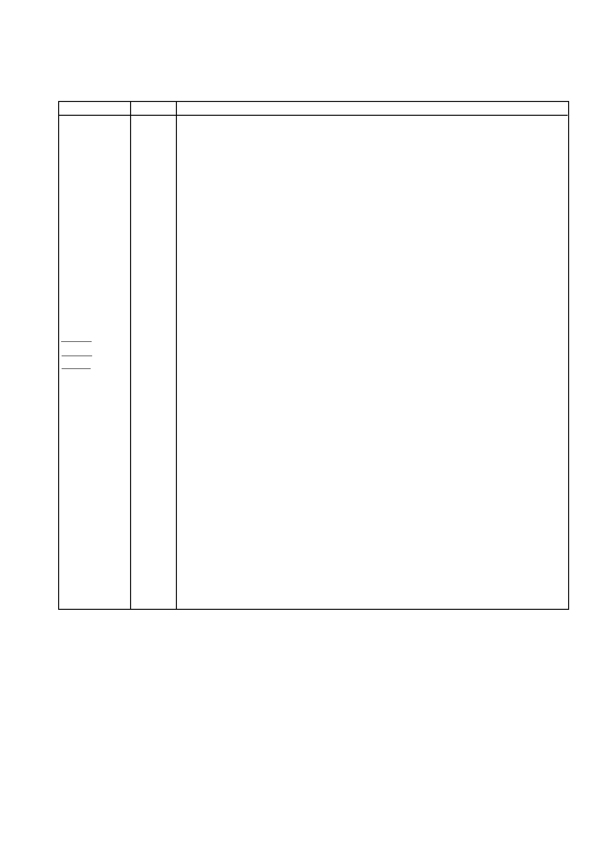
| |||
VP5313/VP5513
PIN DESCRIPTIONS
Pin Name
PD0-7
PXCK
Pin No.
2-4,
38-42
44
SA
SCL
SDA
FC0-2
REFSQ
SCSYNC
PALID
COMPSYNC
CLAMP
18
23
24
12-14
9
8
7
6
5
TTXREQ
17
TTXDATA
19
HSYNC
15
VSYNC
16
RESET
22
VREF
33
RREF
34
DACCOMP
25
CVBS1
32
BLUE/CVBS2
GREEN/Y
RED/C
VDD
AVDD
GND
AGND
31
27
26
1, 11, 20
37,28,30
10,21,43
36,29,35
Description
8 Bit Pixel Data inputs clocked by PXCK. PD0 is the least significant bit. These pins are
internally pulled low.
27MHz Pixel Clock input. The VP5313/VP5513 internally divides PXCK by two to provide the
pixel clock.
Slave address select.
Standard I2C bus serial clock input.
Standard I2C bus serial data input/output.
Field Counter output in master sync mode.
Reference square wave input used only during Genlock mode.
Subcarrier sync input, (synchronises phase quadrant in 4xfsc genlock mode), see fig 6.
PAL IDENT input, controls swinging colour burst phase in PAL genlock mode.
Composite sync pulse output. This is an active low output signal.
The CLAMP output signal is synchronised to COMPSYNC output and indicates the position of
the BURST pulse, (lines 10-263 and 273-525 for NTSC; lines 6-310 and 319-623 for PAL-
B,D,G,I,N(Argentina)).
Teletext Data Request output, requests next line of teletext data.
Teletext Data input.
Horizontal Sync, output in master mode, input in slave mode
Vertical Sync, output in master mode, input in slave mode
Master reset. This is an asynchronous, active low, input signal and must be asserted for a
minimum 200ns in order to reset the VP5313/VP5513.
Voltage reference output. This output is nominally 1·0V and should be decoupled with a
100nF capacitor to GND.
DAC full scale current control. A resistor connected between this pin and GND sets the
magnitude of the video output current. An internal loop amplifier controls a reference current
flowing through this resistor so that the voltage across it is equal to the Vref voltage. This
reference current has a weighting equal to 20.8 LSB’s.
DAC compensation. A 100nF ceramic capacitor must be connected to AVDD.
Composite video output. These are high impedance current source outputs. A DC path to
GND must exist from each of these pins.
Blue or composite DAC output. Output type as CVBS1.
Green or luminance DAC output. Output type as CVBS1.
Red or chrominance DAC output. Output type as CVBS1.
Positive supply input. All VDD pins must be connected.
Analog positive supply input. All AVDD pins must be connected.
Negative supply input. All GND pins must be connected.
Analog negative supply input. All AGND pins must be connected.
4
Share Link: 