CS5112 View Datasheet(PDF) - Cherry semiconductor
Part Name
Description
View to exact match
CS5112
Cherry semiconductor

CS5112 Datasheet PDF : 10 Pages
| |||
Application Notes: continued
Pole due to error amplifier
output impedance and C1
A
fz = 1/2pR4C1
G
B
+G C
error amplifier gain
fP = 1/pR4C2
-20dB/dec
fP = 1/p RLoadCOUT
fCO
0
modulator gain + feedback resistor divider attenuation
-G
fz = 1/2p ESR COUT
Figure 10. Bode plot of error amplifier (OTA) gain and modulator gain
added to the feedback resistor divider attenuation.
A pole at point C:
fp = 1/(¹R4C2),
(8g)
offsets the zero set by the ESR of the output capacitors.
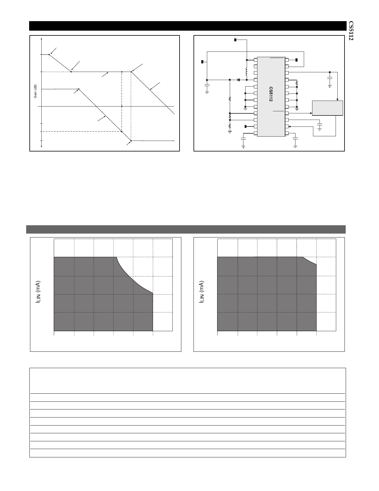
An alternative scheme uses a single capacitor as shown in
Figure 11, to roll the gain off at a relatively low frequency.
VIN
VOUT = 18V, Select > 2V
VOUT = 16V, Select < 0.8V
L=33mH
COUT (2)
88mF
R1 100kW
VIN
NC
NC
VSW
Gnd
ENABLE
VREG
VLIN
IBIAS
Gnd
Gnd
Gnd
Gnd
Gnd
Gnd
Gnd
R2 946W
R3 7.5kW
(1) VFB1
VFB2
RESET
CDelay
SELECT WDI
CCOMP
0.33mF
COMP COSC
5V
100mF
ESR<8W
RBIAS = 64.9kW
MICROPROCESSOR
COSC
390pF
Cdelay
0.1mF
Figure 11. A typical application diagram with external components con-
figured in a boost topology.
Step 9
Finally the watchdog timer period and Power on Reset
time is determined by:
tDelay = 1.353 ´ CDelayRBIAS.
(9)
Linear Regulator Output Current vs. Input Voltage
100
100
75
50
QJA = 55°C/W
VIN = 14V
Max Total Power = 1.18W
25
75
QJA = 35°C/W
50
VIN = 14V
Max Total Power = 1.86W
25
0
0
0
5
10
15
20
25
30
VREG (V)
0
5
10
15
20
25
30
VREG (V)
Figure 12: The shaded area shows the safe operating area of the CS5112 as a function of ILIN, VREG, and QJA. Refer to the table below for typical
loads and voltages.
VREG
VIN
(V)
(V)
20
14
ILIN
(mA)
25
Linear Power
Dissipation
(W)
0.44
Worst Case Switcher
Power Available
(QJA = 55¡C/W)
(W)
0.74
Worst Case Switcher
Power Available
(QJA = 35¡C/W)
(W)
1.42
20
14
50
0.83
0.35
1.03
20
14
75
1.22
*
0.64
20
14
100
1.60
*
0.26
25
14
25
0.60
0.58
1.26
25
14
50
1.11
0.07
0.75
25
14
75
1.62
*
0.24
25
14
100
2.14
*
*
* Subjecting the CS5112 to these conditions will exceed the maximum total power that the part can handle, thereby forcing it into thermal limit.
9
Share Link: