MC12179D View Datasheet(PDF) - LANSDALE Semiconductor Inc.
Part Name
Description
View to exact match
MC12179D Datasheet PDF : 11 Pages
| |||
ML12179
LANSDALE Semiconductor, Inc.
Legacy Applications Information
CI
=
CAMP +
CSTRAY +
C1 +
C1 +
C2
C2
Provided the crystal and associated components are located
immediately next to the IC, thus minimizing the stray capacitance,
the combined value of CAMP and CSTRAY is approximately
5pF. Note that the location of the OSCin and OSCout pins at the
end of the package, facilitates placing the crystal, resistor and the
C1 and C2 capacitors very close to the device. Usually, one of the
capacitors is in parallel with an adjustable capacitor used to trim
the frequency of oscillation. It is important that the total external
(to the IC) capacitance seen by either OSCin or OSCout, be no
greater than 30pF.
In operation, the crystal oscillator will start up with the applica-
tion of power. If the crystal is in a can that is not grounded it is
often possible to monitor the frequency of oscillation by connect-
ing an oscilloscope probe to the can; this technique minimizes
any disturbance to the circuit. If a malfunction is indicated, a high
impedance, low capacitance, FET probe may be connected to
either OSCin or OSCout. Signals typically seen at those points
will be very nearly sinusoidal with amplitudes of roughly 300 to
600 mVpp. Some distortion is inevitable and has little bearing on
the accuracy of the signal going to the phase detector.
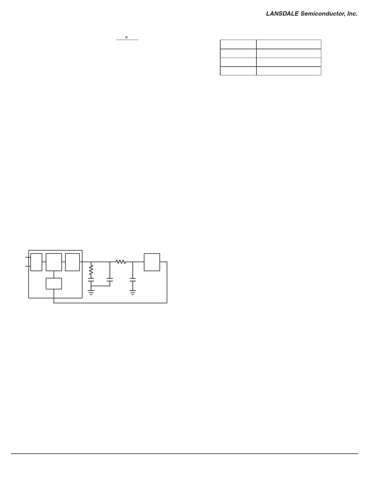
Loop Filter Design
Because the device is designed for a non–frequency agile syn-
thesizer (i.e., how fast it tunes is not critical) the loop filter design
is very straight forward. The current output of the charge pump
allows the loop filter to be realized without the need of any active
components. The preferred topology for the filter is illustrated
below in Figure 5.
Figure 5. Loop Filter
Xtl Ph/Frq Chrg
Osc Det Pump
Kp
256 N
ML12179
VCO
Ro
Rx
Kv
Co
Ca
Cx
The Ro/Co components realize the primary loop filter. Ca is
added to the loop filter to provide for reference sideband suppres-
sion. If additional suppression is needed, the Rx/Cx realizes an
additional filter. In most applications, this will not be necessary.
If all components are used, this results in a 4th order PLL, which
makes analysis difficult. To simplify this, the loop design will be
treated as a 2nd order loop (Ro/Co) and additional guidelines are
provided to minimize the influence of the other components. If
more rigorous analysis is needed, mathematical/system simulation
Component
Ca
Rx
Cx
Guideline
<0.1 x Co
>10 x Ro
<0.1 x Co
tools can be used.
The focus of the design effort is to determine what the loop's
natural frequency, ωo, should be. This is determined by Ro, Co,
Kp, Kv, and N. Because Kp, Kv, and N are given, it is only neces-
sary to calculate values for Ro and Co. There are 3 considerations
in selecting the loop bandwidth:
1) Maximum loop bandwidth for minimum tuning speed
2) Optimum loop bandwidth for best phase noise performance
3)Minimum loop bandwidth for greatest reference sideband
suppression
Usually a compromise is struck between these 3 cases, however,
for the fixed frequency application, minimizing the tuning speed
is not a critical parameter.
To specify the loop bandwidth for optimal phase noise perform-
ance, an understanding of the sources of phase noise in the sys-
tem and the effect of the loop filter on them is required. There are
3 major sources of phase noise in the phase–locked loop – the
crystal reference, the VCO, and the loop contribution. The loop
filter acts as a low–pass filter to the crystal reference and the loop
contribution equal to the total divide–by–N ratio. This is mathe-
matically described in Figure 10. The loop filter acts as a
high–pass filter to the VCO with an in–band gain equal to unity.
This is described in Figure 11. The loop contribution includes the
PLL IC, as well as noise in the system; supply noise, switching
noise, etc. For this example, a loop contribution of 15 dB has
been selected, which corresponds to data in Figure 14.
The crystal reference and the VCO are characterized as
high–order 1/f noise sources. Graphical analysis is used to deter-
mine the optimum loop bandwidth. It is necessary to have noise
plots from the manufacturer. This method provides a straightfor-
ward approximation suitable for quickly estimating the optimal
bandwidth. The loop contribution is characterized as white–noise
or low–order 1/f noise given in the form of a noise factor which
combines all the noise effects into a single value. The phase noise
of the Crystal References increased by the noise factor of the PLL
IC and related circuitry. It is further increased by the total
divide–by–N ratio of the loop. This is illustrated in Figure 6.
The point at which the VCO phase noise crosses the amplified
phase noise of the Crystal Reference is the point of the optimum
loop bandwidth. In the example of Figure 6, the optimum band-
width is approximately 15 KHz.
Page 5 of 11
www.lansdale.com
Issue A
Share Link: 