MC12179D View Datasheet(PDF) - LANSDALE Semiconductor Inc.
Part Name
Description
View to exact match
MC12179D Datasheet PDF : 11 Pages
| |||
ML12179
Legacy Applications Information
LANSDALE Semiconductor, Inc.
The ML12179 is intended for applications where a fixed local
oscillator is required to be synthesized. The prescaler on the
ML12179 operates up to 2.8GHz which makes the part ideal for
many satellite receiver applications as well as applications in the
2nd ISM (Industrial, Scientific, and Medical) band which covers
the frequency range of 2400MHz to 2483MHz. The part is also
intended for MMDS (Multi–channel Multi–point Distribution
System) block downconverter applications. Below is a typical block
diagram of the complete PLL.
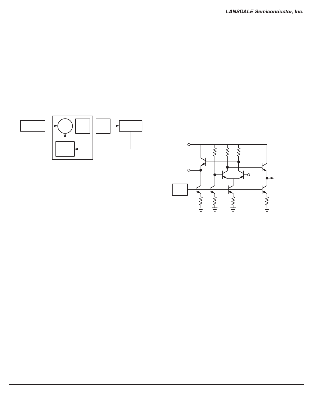
Figure 3. Typical Block Diagram of Complete PLL
External Ref
10.0 MHz
ML12179 PLL
φ/Freq Charge
Loop
Det
Pump
Filter
VCO
2560.00 MHz
Since the ML12179 is realized with an all–bipolar ECL style
design, the internal oscillator circuitry is different from more tradi-
tional CMOS oscillator designs which realize the crystal oscillator
with a modified inverter topology. These CMOS designs typically
excite the crystal with a rail–to–rail signal which may overdrive the
crystal resulting in damage or unstable operation. The ML12179
design does not exhibit these phenomena because the swing out of
the OSCout pin is less than 600mV. This has the added advantage
of minimizing EMI and switching noise which can be generated by
rail–to–rail CMOS outputs. The OSCout output should not be used
to drive other circuitry.
The oscillator buffer in the ML12179 is a single stage, high
speed, differential input/output amplifier; it may be considered to
be a form of the Pierce oscillator. A simplified circuit diagram is
seen in Figure 4.
Figure 4. Simplified Crystal Oscillator/Buffer Circuit
P
VCC
256
As can be seen from the block diagram, with the addition of a
VCO, a loop filter, and either an external oscillator or crystal, a
complete PLL sub–system can be realized. Since most of the PLL
function is integrated into the ML12179, the user's primary focus is
on the loop filter design and the crystal reference circuit. Figure 13
and Figure 14 illustrate typical VCO spectrum and phase noise
characteristics. Figure 17 and Figure 18 illustrate the typical input
impedance versus frequency for the prescaler input.
OSCout
Bias
Source
OSCin
To Phase/
Frequency
Detector
Crystal Oscillator Design
The ML12179 is used as a multiply–by–256 PLL circuit which
transfers the high stability characteristic of a low frequency refer-
ence source to the high frequency VCO in the PLL loop. To facili-
tate this, the device contains an input circuit which can be config-
ured as a crystal oscillator or a buffer for accepting an external sig-
nal source.
In the external reference mode, the reference source is AC–cou-
pled into the OSCin input pin. The input level signal should be
between 500–2200 mVpp. When configured with an external refer-
ence, the device can operate with input frequencies down to 2
MHz, thus allowing the circuit to control the VCO down to 512
MHz. To optimize the phase noise of the PLL when used in this
mode, the input signal amplitude should be closer to the upper
specification limit. This maximizes the slew rate of the input signal
as it switches against the internal voltage reference.
In the crystal mode, an external parallel–resonant fundamental
mode crystal is connected between the OSCin and OSCout pins.
This crystal must be between 5.0 MHz and 11 MHz. External
capacitors, C1 and C2 as shown in Figure 1, are required to set the
proper crystal load capacitance and oscillator frequency. The values
of the capacitors are dependent on the crystal chosen and the input
capacitance of the device and any stray board capacitance.
In either mode, a 50kΩ resistor must be connected between the
OSCin and the OSCout pins for proper device operation. The value
of this resistor is not critical so a 47kΩ or 51kΩ ±10% resistor is
acceptable.
OSCin drives the base of one input of an NPN transistor differ-
ential pair. The non–inverting input of the differential pair is inter-
nally biased. OSCout is the inverted input signal and is buffered by
an emitter follower with a 70 µA pull–down current and has a volt-
age swing of about 600 mVpp. Open loop output impedance is
about 425Ω. The opposite side of the differential amplifier output
is used internally to drive another buffer stage which drives the
phase/frequency detector. With the 50 kΩ feedback resistor in
place, OSCin and OSCout are biased to approximately 1.1V below
VCC. The amplifier has a voltage gain of about 15 dB and a band-
width in excess of 150 MHz. Adherence to good RF design and
layout techniques, including power supply pin decoupling, is
strongly recommended.
A typical crystal oscillator application is shown in Figure 1. The
crystal and the feedback resistor are connected directly between
OSCin and OSCout, while the loading capacitors, C1and C2, are
connected between OSCin and ground, and OSCout and ground
respectively. It is important to understand that as far as the crystal
is concerned, the two loading capacitors are in series (albeit
through ground). So when the crystal specification defines a spe-
cific loading capacitance, this refers to the total external (to the
crystal) capacitance seen across its two pins.
This capacitance consists of the capacitance contributed by the
amplifier (IC and packaging), layout capacitance, and the series
combination of the two loading capacitors. This is illustrated in the
equation below:
Page 4 of 11
www.lansdale.com
Issue A
Share Link: 