AD9100 View Datasheet(PDF) - Analog Devices
Part Name
Description
View to exact match
AD9100 Datasheet PDF : 12 Pages
| |||
AD9100
Hold vs. Track Mode Distortion
In many traditional high speed, open loop track-and-holds,
track mode distortion is often much better than hold mode
distortion. Track mode distortion does not include nonlineari-
ties due to the switch network, and does not correlate to the
relevant hold mode distortion. But since hold mode distortion
has traditionally been omitted from manufacturer’s specification
tables, users have had to discover for themselves the effective
overall hold mode distortion of the combined T/H and encoder.
The architecture of the AD9100 minimizes hold mode distortion
over its specified frequency range. As an example, in track mode
the worst harmonic generated for a 20 MHz input tone is typi-
cally –65 dBfs. In hold mode, under the same conditions
and sampling at 30 MSPS, the worst harmonic generated is
–74 dBfs. The reason is the output buffer in hold mode has only
dc distortion relevancy. With its inherent linearity (7 ns settling
to 0.01%), the output buffer has essentially settled to its dc
distortion level even for track plus hold times as short as 30 ns.
For a traditional open-loop output buffer, the ac (track mode)
and dc (hold mode) distortion levels are often the same.
Droop Rate
Droop rate does not necessarily affect a track and hold’s distor-
tion characteristics. If the droop rate is constant versus the input
voltage for a given hold time, it manifests itself as a dc offset to
the encoder. For the AD9100, the droop rate is typically
± 1 mV/µs. If a signal is held for 1 µs, a subsequent encoder
would see a 1 mV offset voltage. If there is no droop sensitivity
to the held voltage value, the 1 mV offset would be constant
and “ride” on the input signal and introduce no hold-mode
nonlinearities .
In instances in which droop rate varies proportionately to the
magnitude of the held voltage signal level, a gain error only is
introduced to the A/D encoder. The AD9100 has a droop sensi-
tivity to the input level of 1.5 mV/ V–µs. For a 2 V p-p input
signal, this translates to a 0.15%/µs gain error and does not
cause additional distortion errors.
For the AD9100, droop sensitivity to input level is insignificant.
However, hold times longer than about 2 µs can cause distortion due
to the R ϫ CH time constant at the hold capacitor. In addition,
hold mode noise will increase linearly vs. hold time and thus
degrade SNR performance.
Layout Considerations
For best performance results, good high speed design tech-
niques must be applied. The component (top) side ground
plane should be as large as possible; two-ounce copper cladding
is preferable. All runs should be as short as possible, and decou-
pling capacitors must be used.
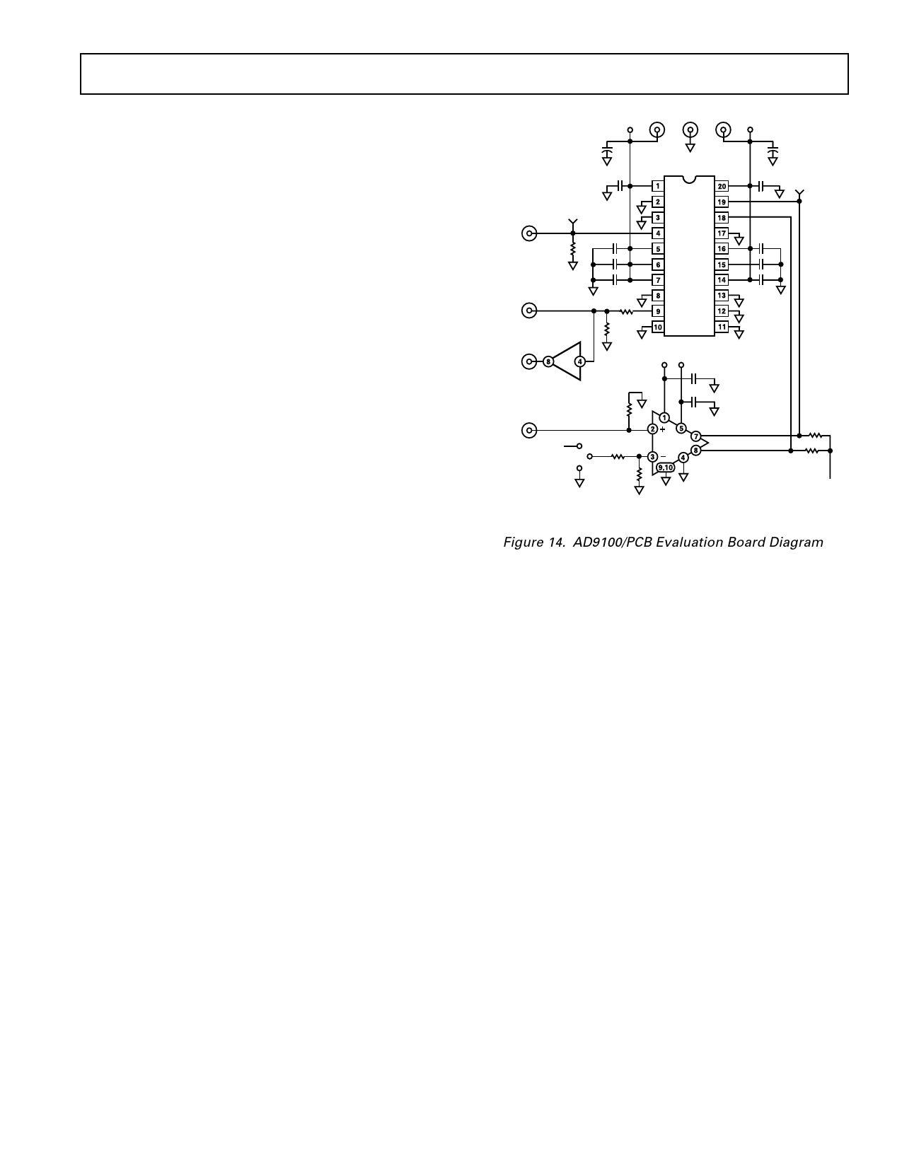
Figure 14 is the schematic of a recommended AD9100 evalua-
tion board. (Contact factory concerning availability of assembled
boards.) All 0.01 µF decoupling capacitors should be low induc-
tance surface mount devices (P/N 05085C103MT050 from
AVX) and connected on the component side within 30 mils of
the designated pins; with the other sides soldered directly to the
top ground plane.
–VS J5
J6
J7 +VS
C14
10F
+ C13
10F
C1
C5 TP3
TP1
J1
VIN
RIN
C2
50⍀
C3
C4
AD9100
C6
DUT
(DIP)
C7
C8
J2
VOUT
J3
VBUFF
RS
5⍀
RL
2k⍀
AD9620
CLOCK
IN
R1
100⍀
+5V
W1
R2
6⍀
W2
R3
4⍀
+VS –VS
C10
C9
Q
AD96685
Q
LE
NOTE:
CONNECT TO W1 FOR TTL CLOCK SIGNALS;
CONNECT TO W2 FOR GROUND-REFERENCED SIGNALS.
R4
510⍀
R5
510⍀
–5.2V
Figure 14. AD9100/PCB Evaluation Board Diagram
The 10 µF low frequency power supply tantalum decoupling
capacitors should be located within 1.5 inches of the AD9100.
The common 0.01 µF supply capacitors can be wired together.
The common power supply bus (connected to the 10 µF capaci-
tor and power supply source) can be routed to the underside of
the board to the daisy chain wired 0.01 µF supply capacitors.
For remote input and/or output drive applications, controlled
impedances are required to minimize line reflections which will
reduce signal fidelity. When capacitive and/or high impedance
levels are present, the load and/or source should be physically
located within approximately one inch of the AD9100. Note
that a series resistance, RS, is required if the load is greater than
6 pF. (The Recommended RS vs. CL chart in the “Typical
Performance Section” shows values of RS for various capacitive
loads which result in no more than a 20% increase in settling
time for loads up to 80 pF.) As much of the ground plane as
possible should be removed from around the VIN and VOUT pins
to minimize coupling onto the analog signal path.
While a single ground plane is recommended, the analog signal
and differential ECL clock ground currents follow a narrow path
directly under their common voltage signal line. To reduce
reflections, especially when terminations are used for transmission
line efficiency, the clock, VIN, and VOUT signals and respective
ground paths should not cross each other; if they do, unwanted
coupling can result.
High current ground transients via the high frequency decou-
pling capacitors can also cause unwanted coupling to the VIN
and VOUT current loops. Therefore, these analog terminations
should be kept as far as possible from the power supply decou-
pling capacitors to minimize feedthrough.
REV. B
–7–
Share Link: 