AD9100 View Datasheet(PDF) - Analog Devices
Part Name
Description
View to exact match
AD9100 Datasheet PDF : 12 Pages
| |||
AD9100
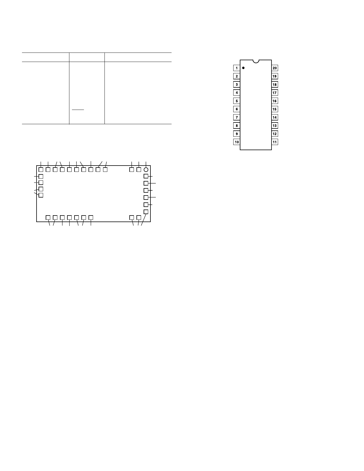
PIN FUNCTION DESCRIPTIONS/CONNECTIONS
Pin No.
1
2, 3, 8, 10–13, 17
4
5, 7
6, 15
9
14, 16, 20
18
19
Description Connection
–VS
GND
VIN
–VS
BYPASS
VOUT
+VS
CLK
CLK
–5.2 V Power Supply
Common Ground Plane
Analog Input Signal
–5.2 V Power Supply
0.1 µF to Ground
Track-and-Hold Output
+5 V, Power Supply
Complement ECL Clock
“True” ECL Clock
CHIP PAD ASSIGNMENTS
+VS +VS
+VS CAP HOLD CAP
NC GND +VS (NOTE 1) (NOTE 3)
+VS +VS NC
13 12 11 10 9 8 7 6 5 4
CLOCK 14
CLOCK 15
16
GND
17
AD9100
TOP VIEW
(Not to scale)
18 19 20 21 22 23 24
32 1
32
31
30
29
28
27
25 26
+VS
BYPASS
(NOTE 2)
+VOUT
BYPASS
(NOTE 2)
+VS
–VS NC –VIN –VS –VS CAP
–VS
(NOTE 1)
SIZE = 148 ؋ 63 ؋ 15 mils NC = NO CONNECT
NOTES:
1. SUPPLY BYPASS CAPACITOR; 0.01 TO 0.1F CERAMIC
CONNECTED TO GROUND.
2. 0.01F CERAMIC CONNECTED BETWEEN PAD 29 AND PAD 31.
3. HOLD CAPACITOR CONNECTED FROM PAD 4 AND PAD 5 TO
GROUND; 10–100pF, NOMINALLY 22pF. DIP PACKAGE DOES NOT
REQUIRE EXTERNAL HOLD CAPACITOR.
PIN CONFIGURATION
20-Lead Side-Brazed Ceramic DIP
–VS
GND
GND
VIN
–VS
BYPASS
–VS
GND
VOUT
GND
AD9100
TOP VIEW
(Not to Scale)
+VS
CLK
CLK
GND
+VS
BYPASS
+VS
GND
GND
GND
TERMINOLOGY
Analog Delay is the time required for an analog input signal to
propagate from the device input to output.
Aperture Delay tells when the input signal is actually sampled.
It is the time difference between the analog propagation delay of
the front-end buffer and the control switch delay time. (The
time from the hold command transition to when the switch is
opened.) For the AD9100, this is a positive value which means
that the switch delay is longer than the analog delay.
Aperture Jitter is the random variation in the aperture delay.
This is measured in ps-rms and results in phase noise on the
held signal.
Droop Rate is the change in output voltage as a function of
time (dV/dt). It is measured at the AD9100 output with the
device in hold mode and the input held at a specified dc value,
the measurement starts immediately after the T/H switches from
track to hold. Feedthrough Rejection is the ratio of the input
signal to the output signal when in hold mode. This is a mea-
sure of how well the switch isolates the input signal from feeding
through to the output.
Hold-to-Track Switch Delay is the time delay from the track
command to the point when the output starts to change and
acquire a new signal.
Pedestal Offset is the offset voltage step measured immediately
after the AD9100 is switched from track to hold with the input
held at zero volts. It manifests itself as an added offset during
the hold time.
Track-to-Hold Settling Time is the time necessary for the
track to hold switching transient to settle to within 1 mV of its
final value.
Track-to-Hold Switching Transient is the maximum peak
switch induced transient voltage which appears at the AD9100
output when it is switched from track to hold.
–4–
REV. B
Share Link: 