AD9100AD(RevA) View Datasheet(PDF) - Analog Devices
Part Name
Description
View to exact match
AD9100AD Datasheet PDF : 12 Pages
| |||
AD9100
While a single ground plane is recommended, the analog signal Driving the Analog Input
and differential ECL clock ground currents follow a narrow path Special care must be taken to ensure that the analog input signal
directly under their common voltage signal line. To reduce re-
is not compromised before it reaches the AD9100. To obtain
flections, especially when terminations are used for transmission maximum signal to noise performance, a very low phase noise
line efficiency, the clock, VIN, and VOUT signals and respective
ground paths should not cross each other; if they do, unwanted
analog source is required. In addition, input filtering and/or a
low harmonic signal source is necessary to maximize the
coupling can result.
spurious free dynamic range. Any required filtering should be
High current ground transients via the high frequency decou-
done close to the AD9100 and away from any digital lines.
pling capacitors can also cause unwanted coupling to the VIN
and VOUT current loops. Therefore, these analog terminations
should be kept as far as possible from the power supply decou-
Overdriving the Analog Input
The AD9100 has input clamps that prevent hard saturation of
the output buffer, thereby providing fast overvoltage recovery
pling capacitors to minimize feedthrough.
when the analog input transitions to the linear region (± 2 V).
Using Sockets
The clamps are set internally at ± 2.3 V and cannot be altered by
OBSOLETE Pin sockets (P/N 6-330808-3 from AMP) should be used if the
device can not be soldered directly to the PCB. High profile or
wire wrap type sockets will dramatically reduce the dynamic
performance of the device in addition to increasing the case-to-
ambient thermal resistance.
Driving the Encode Clock
The AD9100 requires a differential ECL clock command. Due
to the high gain bandwidth of the AD9100 internal switch, the
input clock should have a slew rate of at least 100 V/µs.
To obtain maximum signal to noise performance, especially at
high analog input frequencies, a low jitter clock source is
required. The AD9100 clock can be driven by an AD96685, an
ultrahigh speed ECL comparator with very low jitter.
150
CLK 19
150
18 CLK
the user. The output settles to 0.1% of its value 21 ns after the
overvoltage condition is alleviated. When the analog input is
outside the linear region, the analog output will be at either
+2.2 V or –2.2 V.
Matching the AD9100 to A/D Encoders
The AD9100’s analog output level may have to be offset or
amplified to match the full-scale range of a given A/D converter.
This can generally be accomplished by inserting an amplifier
after the AD9100. For example, the AD671 is a 12-bit 500 ns
monolithic ADC encoder that requires a 0 to +5 V full-scale
analog input. An AD84X series amplifier could be used to
condition the AD9100 output to match the full-scale range of
the AD671.
Ultralow Distortion/Low Resistive Load Applications
When driving low resistive loads or when the widest possible
spurious free dynamic range is required, system performance
can be improved by isolating the load from the AD9100. (See
1k
1k
Figure 3.) The AD9620 low distortion closed-loop buffer
amplifier has an input resistance of 800 kΩ and generates
–5.2V
–5.2V
Clock/Clock Input Stage
J5
–VS
J6
J7
+VS
harmonics that are less than those generated by the AD9100.
Other buffers should not be considered if their harmonics are
not lower than those of the AD9100.
C14
10µF
C1
TP1
J1
VIN
RIN
C2
50 Ω
C3
C4
J3
VBUFF
J2
VOUT
8
4
AD9620
RS
5Ω
RL
2kΩ
1
20
2
19
3
18
4
AD9100
17
5
DUT
16
6
(DIP)
15
7
14
8
13
9
12
10
11
+VS –VS
C10
C13
10µF
C5
TP3
C6
C7
C8
ANALOG
INPUT
AD9100
AD9620
INTO LOW
RESISTIVE
LOAD
Figure 3. Using AD9620 as Isolation Amplifier
Direct IF Conversion
The AD9100 can be used to sample super-Nyquist signals,
making wide dynamic range direct IF to digital conversion
practical. By reducing the analog input level to the track and
hold, distortion due to the AD9100 can be minimized. As the
input level is reduced, the gain in the output amplifier (see
Figure 4) must be increased to match the full scale level of the
subsequent analog to digital converter.
R1
CLOCK 100Ω
IN
R2
+5V
W1 68 Ω
W2
R3
47Ω
C9
1
2
5
Q
7
AD96685
Q
3
8
4
9,10 LE
NOTE:
CONNECT TO W1 FOR TTL CLOCK SIGNALS;
CONNECT TO W2 FOR GROUND-REFERENCED SIGNALS.
R4
510Ω
R5
510Ω
–5.2V
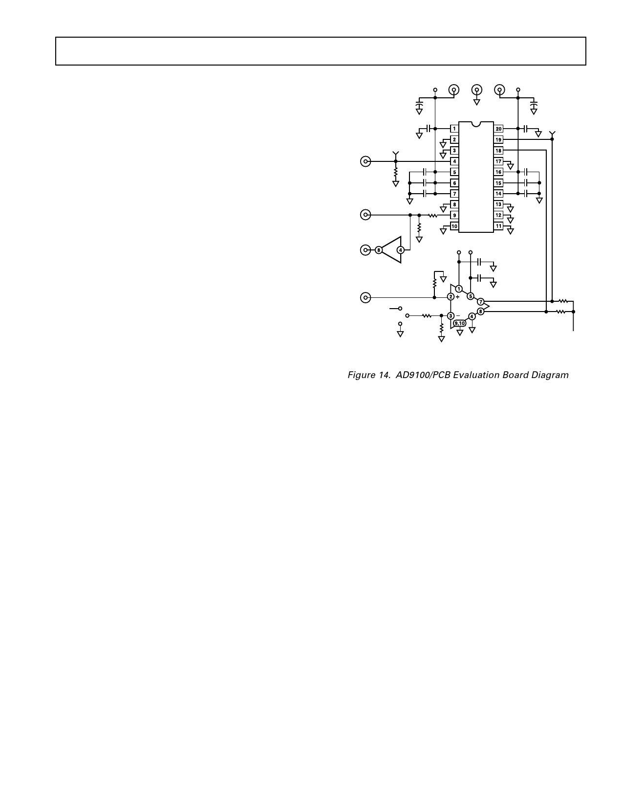
Figure 2. AD9100/PCB Evaluation Board Diagram
REV. A
–7–
Share Link: 