AD9100AD(RevA) View Datasheet(PDF) - Analog Devices
Part Name
Description
View to exact match
AD9100AD Datasheet PDF : 12 Pages
| |||
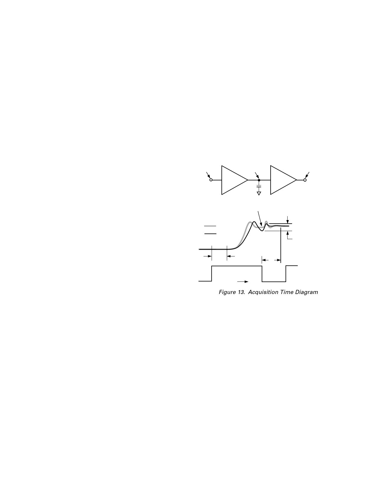
AD9100
VIN
VCH
INPUT
BUFFER
CH
OUTPUT
BUFFER
VOUT
–74 dBfs. The reason is the output buffer in hold mode has only
dc distortion relevancy. With its inherent linearity (7 ns settling
to 0.01%), the output buffer has essentially settled to its dc
distortion level even for track plus hold times as short as 30 ns.
For a traditional open-loop output buffer, the ac (track mode)
and dc (hold mode) distortion levels are often the same.
Droop Rate
ACQUISITION TIME
AT CH TO X%
Droop rate does not necessarily affect a track and hold’s distor-
tion characteristics. If the droop rate is constant versus the input
voltage for a given hold time, it manifests itself as a dc offset to
the encoder. For the AD9100, the droop rate is typically
VCH
± 1 mV/µs. If a signal is held for 1 µs, a subsequent encoder
VOUT
PEAK TRANSIENT
would see a 1 mV offset voltage. If there is no droop sensitivity
OBSOLETE tDHT
6ns
TRACK
TIME
SEEN BY OUTPUT
BUFFER
tS
HOLD
Figure 1. Acquisition Time Diagram
The exaggerated illustration in Figure 1 shows that VCH has
settled to within x% of its final value, but VOUT (due to slew rate
limitations, finite BW, power supply ringing, etc.) has not
settled during the track time. However, since the output buffer
always “tracks” the front end circuitry, it “catches up” during
the hold time and directly superimposes itself (less about 600 ps
of analog delay) to VCH. Since the small-signal settling time of
to the held voltage value, the 1 mV offset would be constant
and “ride” on the input signal and introduce no hold-mode
nonlinearities .
In instances in which droop rate varies proportionately to the
magnitude of the held voltage signal level, a gain error only is
introduced to the A/D encoder. The AD9100 has a droop sensi-
tivity to the input level of 1.5 mV/ V–µs. For a 2 V p-p input sig-
nal, this translates to a 0.15%/µs gain error and does not cause
additional distortion errors.
For the AD9100, droop sensitivity to input level is insignificant.
However, hold times longer than about 2 µs can cause distortion due
to the R ϫ CH time constant at the hold capacitor. In addition,
hold mode noise will increase linearly vs. hold time and thus de-
grade SNR performance.
Layout Considerations
For best performance results, good high speed design tech-
the output buffer is about 1.8 ns to ± 1 mV and is significantly
niques must be applied. The component (top) side ground
less than the specified hold time, acquisition time should be
plane should be as large as possible; two-ounce copper cladding
referenced to the hold capacitor.
is preferable. All runs should be as short as possible, and decou-
Note that most of the hold settling time and output acquisition
pling capacitors must be used.
time are due to the input buffer and the switch network. For
Figure 2 is the schematic of a recommended AD9100 evaluation
track time, the output buffer contributes only about 5 ns of the board. (Contact factory concerning availability of assembled
total; in hold mode, it contributes only 1.8 ns (as stated above). boards.) All 0.01 µF decoupling capacitors should be low
A stricter definition of acquisition time would total the acquisi-
tion and hold times to a defined accuracy. To obtain 12 bit +
distortion levels and 30 MSPS operation, the recommended
track and hold times are 20 ns and 13.5 ns, respectively. To
inductance surface mount devices (P/N 05085C103MT050
from AVX) and connected on the component side within 30
mils of the designated pins; with the other sides soldered
directly to the top ground plane.
drive an 8-bit flash converter with a 2 V p-p full-scale input,
The 10 µF low frequency power supply tantalum decoupling
hold time to 1 LSB accuracy will be limited primarily by the
capacitors should be located within 1.5 inches of the AD9100.
encoder, rather than by the AD9100. This makes it possible to
The common 0.01 µF supply capacitors can be wired together.
reduce track time to approximately 13 ns, with hold time chosen The common power supply bus (connected to the 10 µF
to optimize the encoder’s performance.
capacitor and power supply source) can be routed to the
Hold vs. Track Mode Distortion
In many traditional high speed, open loop track-and-holds,
underside of the board to the daisy chain wired 0.01 µF supply
capacitors.
track mode distortion is often much better than hold mode dis- For remote input and/or output drive applications, controlled
tortion. Track mode distortion does not include nonlinearities
impedances are required to minimize line reflections which will
due to the switch network, and does not correlate to the relevant reduce signal fidelity. When capacitive and/or high impedance
hold mode distortion. But since hold mode distortion has tradi- levels are present, the load and/or source should be physically
tionally been omitted from manufacturer’s specification tables, located within approximately one inch of the AD9100. Note
users have had to discover for themselves the effective overall
that a series resistance, RS, is required if the load is greater than
hold mode distortion of the combined T/H and encoder.
6 pF. (The Recommended RS vs. CL chart in the “Typical
The architecture of the AD9100 minimizes hold mode distortion
over its specified frequency range. As an example, in track mode
the worst harmonic generated for a 20 MHz input tone is
typically –65 dBfs. In hold mode, under the same conditions
and sampling at 30 MSPS, the worst harmonic generated is
Performance Section” shows values of RS for various capacitive
loads which result in no more than a 20% increase in settling
time for loads up to 80 pF.) As much of the ground plane as
possible should be removed from around the VIN and VOUT pins
to minimize coupling onto the analog signal path.
–6–
REV. A
Share Link: 