VP5513A View Datasheet(PDF) - Mitel Networks
Part Name
Description
View to exact match
VP5513A Datasheet PDF : 19 Pages
| |||
VP5313/VP5513
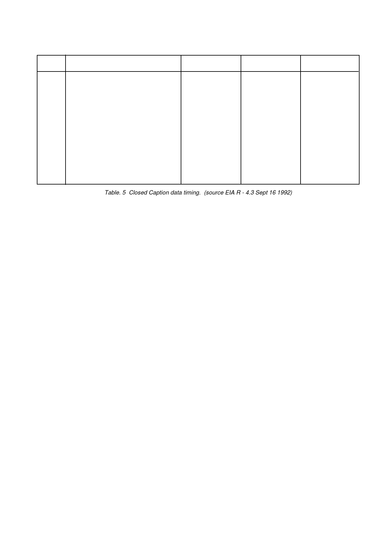
Interval
Description
Encoder minimum Encoder nominal Encoder maximum
A
H-sync to clock run-in
B
Clock run-in 2, 3
C
Clock run-in to third start bit 3
D
Data bit 1, 3
E
Data characters 4
H
Horizontal line 1
Rise / fall time of data bit transitions 5
Data bit high (logic level one) 6
Clock run-in maximum
Data bit low (logic level zero) 6
Clock run-in minimum
Data bit differential (high - low)
Clock run-in differential (max. - min)
10.250µs
48 IRE
0 IRE
48 IRE
10.500µs
6.5D (12.910µs)
2.0D (3.972µs)
1.0D (1.986µs)
16.0D (31.778µs)
32.0D (63.556)
0.240µs
50 IRE
0 IRE
50 IRE
10.750µs
0.288µs
52 IRE
2 IRE
52 IRE
Table. 5 Closed Caption data timing. (source EIA R - 4.3 Sept 16 1992)
Notes
1. The Horizontal line frequency fH is nominally 15734.26Hz ±0.05Hz. Interval D shall be adjusted to D = 1/(fH x 32) for the
instantaneous fH at line 21.
2. The clock run-in signal consists of 7.0 cycles of a 0.5034965MHz (1/D) sine wave when measured from the leading to trailing
0 IRE points. The sine wave is to be symmetrical about the 25 IRE level.
3. The negative going midpoints (half amplitude) of the clock run-in shall be coherent with the midpoints (half amplitude) of the
Start and Data bit transitions.
4. Two characters, each consisting of 7 data bits and 1 odd parity bit.
5. 2 T Bar, measured between the 10% and 90% amplitude points.
6. The clock run-in maximum level shall not differ from the data bit high level by more than ±1 IRE. The clock run-in minimum
level shall not differ from the data bit low level by more than ±1 IRE.
14
Share Link: 