72605L20 View Datasheet(PDF) - Integrated Device Technology
Part Name
Description
View to exact match
72605L20 Datasheet PDF : 20 Pages
| |||
IDT72605/IDT72615 CMOS SyncBiFIFO
256 x 18 x 2 and 512 x 18 x 2
AC TEST CONDITIONS
In Pulse Levels
Input Rise/Fall Times
Input Timing Reference Levels
Output Reference Levels
Output Load
GND to 3.0V
3ns
1.5V
1.5V
See Figure 2
2704 tbl 07
COMMERCIAL TEMPERATURE RANGE
+5V
D.U.T.
680Ω
1.1KΩ
30pF*
2704 drw 05
AC ELECTRICAL CHARACTERISTICS
(Commercial: VCC = 5V±10%, TA = 0°C to +70°C)
Symbol
fCLK
tCLK
tCLKH
tCLKL
tRS
tRSS
tRSR
tRSF
tA
tCS
Parameter
Clock frequency
Clock cycle time
Clock HIGH time
Clock LOW time
Reset pulse width
Reset set-up time
Reset recovery time
Reset to flags in intial state
Data access time
Control signal set-up time(1)
tCH
Control signal hold time(1)
72615L20
72605L20
Min. Max.
—
50
20
—
8
—
8
—
20
—
12
—
12
—
—
27
3
10
6
—
1
—
tDS
Data set-up time
6
—
tDH
Data hold time
1
—
tOE
Output Enable LOW to
output data valid(2)
3
10
tOLZ Output Enable LOW to data
bus at Low-Z(2)
0
—
tOHZ Output Enable HIGH to data
bus at High-Z(2)
3
10
tFF
Clock to Full Flag time
— 10
tEF
Clock to Empty Flag time
—
10
tPAE Clock to Programmable
Almost Empty Flag time
—
12
tPAF Clock to Programmable
Almost Full Flag time
—
12
tSKEW1
Skew between CLKA & CLKB
for Empty/Full Flags(2)
10
—
tSKEW2
Skew between CLKA & CLKB
for Programmable Flags(2)
17
—
NOTES:
1. Control signals refer to CSA, R/WA, ENA, A2, A1, A0, R/WB, ENB.
2. Minimum values are guaranteed by design.
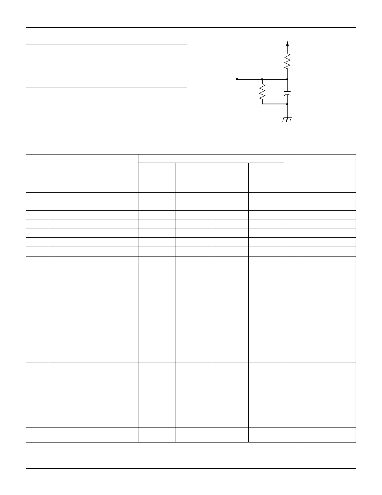
or equivalent circuit
Figure 2. Output Load
* Includes jig and scope capacitances.
Commercial
72615L25 72615L35 72615L50
72605L25 72605L35 72605L50
Min. Max. Min. Max. Min. Max. Unit
— 40 — 28 —
20 MHz
25 — 35 — 50
— ns
10 — 14 — 20
— ns
10 — 14 — 20
— ns
25 — 35 — 50
— ns
15 — 21 — 30
— ns
15 — 21 — 30
— ns
— 28 — 35 —
50 ns
3 15 3 21 3
25 ns
6
—
8
— 10
— ns
1
—
1
—1
— ns
6
—
8
— 10
— ns
1
—
1
—1
— ns
3 13 3 20 3
28 ns
Timing Figures
—
4,5,6,7
4,5,6,7,12,13,14,15
4,5,6,7,12,13,14,15
3
3
3
3
5,7,8,9,10,11
4,5,6,7,8,9,10,11,
12, 13,14,15
4,5,6,7,10,11,12,
13, 14,15
4,6,8,9,10,11
4,6
5,7,8,9,10,11
0
—
0
—0
— ns
5,7,8,9,10,11
3 13 3 20 3
28 ns
5,7,10,11
— 15 — 21 —
— 15 — 21 —
— 15 — 21 —
30 ns
30 ns
30 ns
4,6,10,11
5,7,8,9,10,11
12,14
— 15 — 21 —
30 ns
13,15
12 — 17 — 20
— ns 4,5,6,7,8,9,10,11
19 — 25 — 34
— ns
4, 7,12,13,14,15
2704 tbl 08
5.18
6
Share Link: 