72605L20 View Datasheet(PDF) - Integrated Device Technology
Part Name
Description
View to exact match
72605L20 Datasheet PDF : 20 Pages
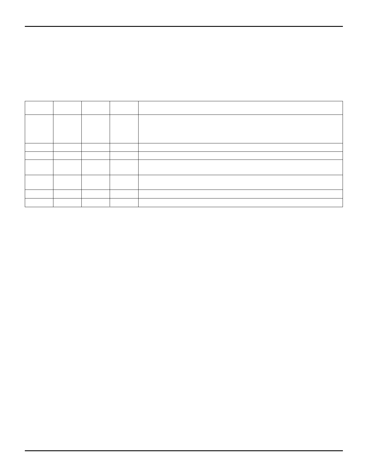
| |||
IDT72605/IDT72615 CMOS SyncBiFIFO
256 x 18 x 2 and 512 x 18 x 2
input register and the FIFO memory. If R/WB is HIGH and OEB
is LOW, data comes out of bus and is read from output register
into three-state buffer. In bypass mode, if R/WB is LOW,
bypass messages are transferred into B→A output register. If
R/WA is HIGH, bypass messages are transferred into A→B
output register. Refer to pin descriptions for more information.
COMMERCIAL TEMPERATURE RANGE
R/WB
ENB
Data B
OEB
I/O
Port B Operation
0
0
0
I
Data B is written on CLKB ↑. This write cycle immediately following output low-
impedance cycle is prohibited. Note that even though OEB = 0, a LOW logic level on
R/WB, once qualified by a rising edge on CLKB, will put Data B into a high-impedance
state.
0
0
1
I
Data B is written on CLKB ↑.
0
1
X
I
Data B is ignored
1
0
0
O
Data is read(1) from RAM array to output register on CLKB ≠, Data B is LOW
impedance
1
0
1
O
Data is read(1) from RAM array to output register on CLKB ≠, Data B is HIGH
impedance
1
1
0
O
Output register does not change(2), Data B is low-impedance
1
1
1
O
Output register does not change(2), Data B is high-impedance
NOTES:
2704 tbl 13
1. When A2A1A0 = 000 or 1XX, the next A→B FIFO value is read out of the output register and the read pointer advances. If A2A1A0 = 001, the bypass
path is selected and bypass data is read from the Port B output register.
2. Regardless of the condition of A2A1A0, the data in the Port B output register does not change and the A→B read pointer does not advance.
Table 5. Port B Operation Control Signals.
5.18
10
Share Link: 