IDT72605(2013) View Datasheet(PDF) - Integrated Device Technology
Part Name
Description
View to exact match
IDT72605 Datasheet PDF : 17 Pages
| |||
IDT72605/72615 CMOS SYNCBiFIFO™
256 x 18x 2 and 512 x 18 x 2
INDUSTRIAL TEMPERATURE RANGE
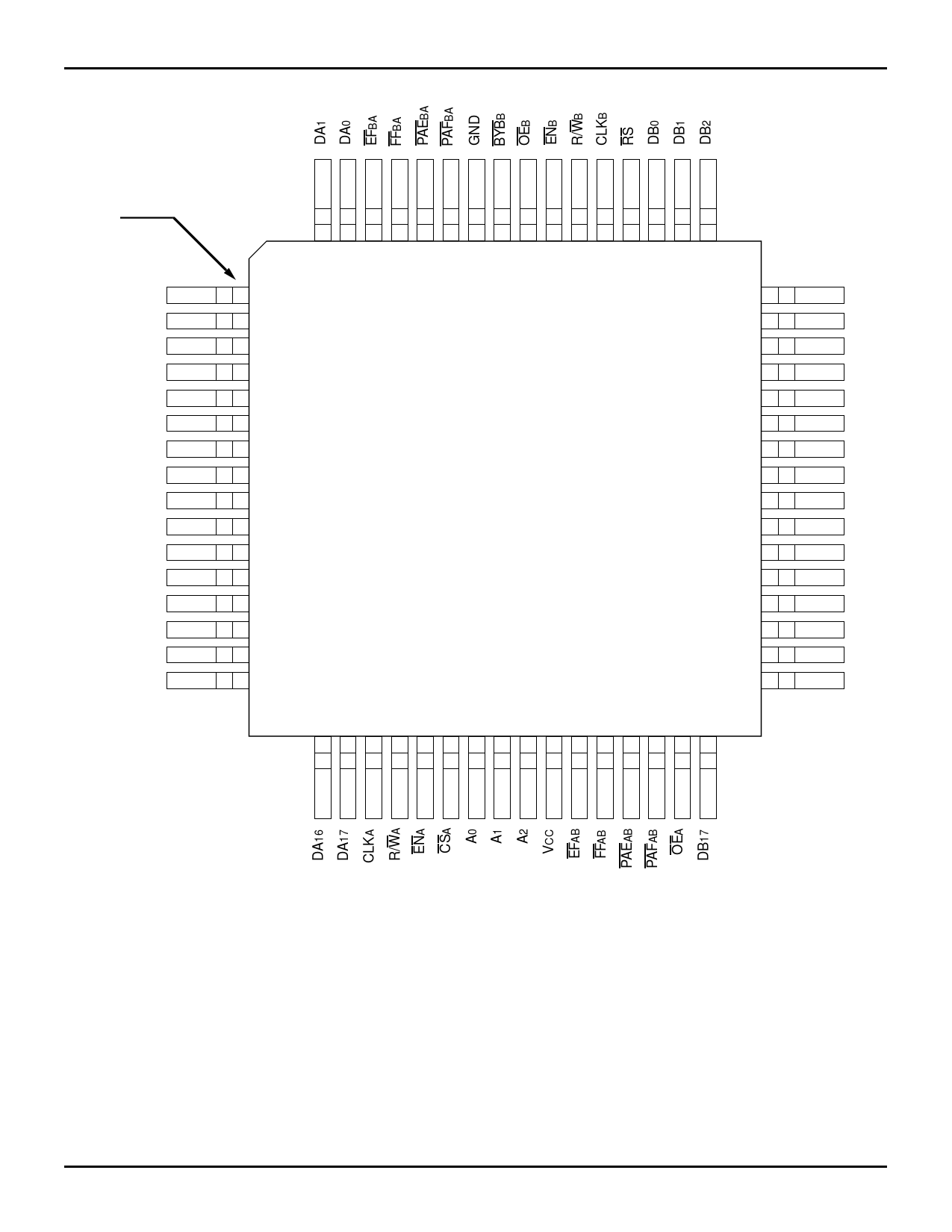
PIN DESCRIPTION
Symbol
Name
I/O
Description
DA0-DA17 Data A
I/O Data inputs & outputs for the 18-bit Port A bus.
CSA
Chip Select A I Port A is accessed when CSA is LOW. Port A is inactive if CSA is HIGH.
R/WA
Read/Write A
I This pin controls the read or write direction of Port A. If R/WA is LOW, Data A input data is written into Port A. If R/WA is HIGH,
Data A output data is read from Port A. In bypass mode, when R/WA is LOW, message is written into A→B output register. If
R/WA is HIGH, message is read from B→A output register.
CLKA Clock A
I CLKA is typically a free running clock. Data is read or written into Port A on the rising edge of CLKA.
ENA
Enable A
I When ENA is LOW, data can be read or written to Port A. When ENA is HIGH, no data transfers occur.
OEA
Output Enable A I When R/WA is HIGH, Port A is an output bus and OEA controls the high-impedance state of DA0-DA17. If OEA is HIGH, Port A is
in a high-impedance state. If OEA is LOW while CSA is LOW and R/WA is HIGH, Port A is in an active (low-impedance) state.
A0, A1, A2 Addresses
I When CSA is asserted, A0, A1, A2 and R/WA are used to select one of six internal resources.
DB0-DB17 Data B
I/O Data inputs & outputs for the 18-bit Port B bus.
R/WB
Read/Write B
I This pin controls the read or write direction of Port B. If R/WB is LOW, Data B input data is written into Port B. If R/WB is HIGH,
Data B output data is read from Port B. In bypass mode, when R/WB is LOW, message is written into B→A output register. If
R/WB is HIGH, message is read from A→B output register.
CLKB Clock B
I Clock B is typically a free running clock. Data is read or written into Port B on the rising edge of CLKB.
ENB
Enable B
I When ENB is LOW, data can be read or written to Port B. When ENB is HIGH, no data transfers occur.
OEB
Output Enable B I When R/WB is HIGH, Port B is an output bus and OEB controls the high-impedance state of DB0-DB17. If OEB is HIGH, Port B is
in a high-impedance state. If OEB is LOW while R/WB is HIGH, Port B is in an active (low-impedance) state.
EFAB
A→B Empty O When EFAB is LOW, the A→B FIFO is empty and further data reads from Port B are inhibited. When EFAB is HIGH, the FIFO is
Flag
not empty. EFAB is synchronized to CLKB. In the bypass mode, EFAB HIGH indicates that data DA0-DA17 is available for passing
through. After the data DB0-DB17 has been read, EFAB goes LOW.
PAEAB
A→B
Programmable
Almost-Empty
Flag
O When PAEAB is LOW, the A→B FIFO is almost-empty. An almost-empty FIFO contains less than or equal to the offset
programmed into PAEAB Register. When PAEAB is HIGH, the A→B FIFO contains more than offset in PAEAB Register. The
default offset value for PAEAB Register is 8. PAEAB is synchronized to CLKB.
PAFAB
A→B
Programmable
Almost-Full
Flag
O When PAFAB is LOW, the A→B FIFO is almost-full. An almost-full FIFO contains greater than the FIFO depth minus the offset
programmed into PAFAB Register. When PAFAB is HIGH, the A→B FIFO contains less than or equal to the depth minus the
offset in PAFAB Register. The default offset value for PAFAB Register is 8. PAFAB is synchronized to CLKA.
FFAB
A→B Full Flag O When FFAB is LOW, the A→B FIFO is full and further data writes into Port A are inhibited. When FFAB is HIGH, the FIFO is not
full. FFAB is synchronized to CLKA. In bypass mode, FFAB tells Port A that a message is waiting in Port B’s output register. If
FFAB is LOW, a bypass message is in the register. If FFAB is HIGH, Port B has read the message and another message can be
written into Port A.
EFBA
B→A Empty O When EFBA is LOW, the B→A FIFO is empty and further data reads from Port A are inhibited. When EFBA is HIGH, the FIFO
Flag
is not empty. EFBA is synchronized to CLKA. In the bypass mode, EFBA HIGH indicates that data DB0-DB17 is available for
passing through. After the data DA0-DA17 has been read, EFBA goes LOW on the following cycle.
PAEBA
B→A
Programmable
Almost-Empty
Flag
O When PAEBA is LOW, the B→A FIFO is almost-empty. An almost-empty FIFO contains less than or equal to the offset
programmed into PAEBA Register. When PAEBA is HIGH, the B→A FIFO contains more than offset in PAEBA Register. The
default offset value for PAEBA Register is 8. PAEBA is synchronized to CLKA.
PAFBA
B→A
Programmable
Almost-Full
Flag
O When PAFBA is LOW, the B→A FIFO is almost-full. An almost-full FIFO contains greater than the FIFO depth minus the offset
programmed into PAFBA Register. When PAFBA is HIGH, the B→A FIFO contains less than or equal to the depth minus the
offset in PAFBA Register. The default offset value for PAFBA Register is 8. PAFBA is synchronized to CLKB.
FFBA
B→A Full Flag O When FFBA is LOW, the B→A FIFO is full and further data writes into Port B are inhibited. When FFBA is HIGH, the FIFO is
not full. FFBA is synchronized to CLKB. In bypass mode, FFBA tells Port B that a message is waiting in Port A’s output register. If
FFBA is LOW, a bypass message is in the register. If FFBA is HIGH, Port A has read the message and another message can be
written into Port B.
BYPB
Port B Bypass O This flag informs Port B that the synchronous BiFIFO is in bypass mode. When BYPB is LOW, Port A has placed the FIFO into
Flag
bypass mode. If BYPB is HIGH, the synchronous BiFIFO passes data into memory. BYPB is synchronized to CLKB.
RS
Reset
I A LOW on this pin will perform a reset of all synchronous BiFIFO functions.
VCC
Power
There are three +5V power pins for the PLCC and two for the TQFP.
GND
Ground
There are seven ground pins for the PLCC and four for the TQFP.
3
Share Link: 